- 您現(xiàn)在的位置:買賣IC網(wǎng) > PDF目錄192292 > S19237PB13 (APPLIEDMICRO INC) TRANSCEIVER, PBGA255 PDF資料下載
參數(shù)資料
| 型號(hào): | S19237PB13 |
| 廠商: | APPLIEDMICRO INC |
| 元件分類: | 數(shù)字傳輸電路 |
| 英文描述: | TRANSCEIVER, PBGA255 |
| 封裝: | PLASTIC, BGA-255 |
| 文件頁數(shù): | 26/60頁 |
| 文件大小: | 1418K |
| 代理商: | S19237PB13 |
第1頁第2頁第3頁第4頁第5頁第6頁第7頁第8頁第9頁第10頁第11頁第12頁第13頁第14頁第15頁第16頁第17頁第18頁第19頁第20頁第21頁第22頁第23頁第24頁第25頁當(dāng)前第26頁第27頁第28頁第29頁第30頁第31頁第32頁第33頁第34頁第35頁第36頁第37頁第38頁第39頁第40頁第41頁第42頁第43頁第44頁第45頁第46頁第47頁第48頁第49頁第50頁第51頁第52頁第53頁第54頁第55頁第56頁第57頁第58頁第59頁第60頁
32
DS1454
AMCC Confidential and Proprietary
S19237 – SONET STS-192/10GbE CMOS Transceiver
with ISI Compensation
Data Sheet
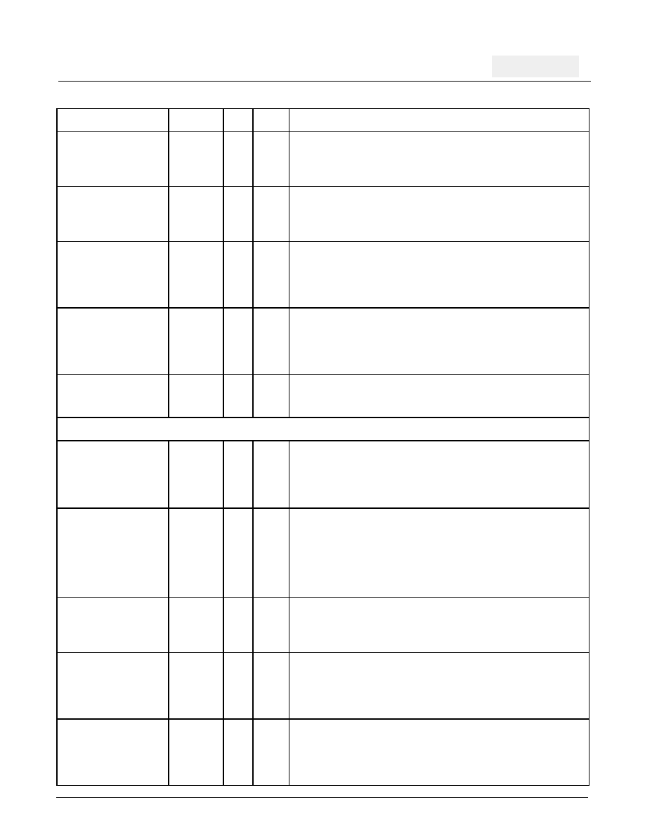
KILLMCKCLKB
MDIO
I
Kill RX_622MCK Clock Output. Active low. For normal operation,
KILLMCKCLKB is high. When this input is low, it will force the
RX_622MCK output to a logic ‘0’ state. This signal can be accessed
through the MDIO bus register (Default = 1).
KILLPOCLKB
MDIO
I
Kill POCLK Output. Active low. For normal operation, KILLPOCLKB
is high. When this input is low, it will force the POCLK output to a
logic ‘0’ state. This signal can be accessed through the MDIO bus
register (Default = 1).
RX_BIST_EN
MDIO
I
Receive Built-In Self Test Enable. This active high input enables
the receive built-in self test mode. In this mode the PRBS generator
will start sending the pattern through the parallel data output and
receive checker will be activated. This signal can be accessed
through the MDIO bus register (Default = 0).
RX_BIST_CLR
MDIO
I
Receive Built-In Self Test Clear. This active high level sensitive
input clears the receive built-in self test error. The RX_BIST_ERR
flag can be cleared by asserting RX_BIST_CLR high in the BIST
mode or by resetting (RSTB) the S19237. This signal can be
accessed through the MDIO bus register (Default = 0).
RXPD
MDIO
I
Receiver Power Down. This active high control input powers down
the CRU and receiver path. This signal can be accessed through the
MDIO bus register (Default = 0).
COMMON INPUTS
RSTB
LVCMOS
Pull Up
I
G13
Master Reset. Reset input for the S19237. Must remain low for 100
ns to accurately reset the transmitter. During reset, PCLK does not
toggle. For normal operation, connect to
VDD_1.8 V. For normal sys-
tem power sequencing on power-up, no reset is required. This signal
can be accessed through an external pin (Default = 1).
DATA_SWAP
MDIO
I
Parallel Input and Output Data Bus Reversal. Reverses the order
of the parallel input and output data bus (PINP/N[15:0] and POUTP/
N[15:0]). DATA_SWAP input should be programmed to logic low
when S19237 is used with 300-pin MSA connector. DATA_SWAP
input should be programmed to logic high when S19237 is used with
200-pin MSA connector. This signal can be accessed through the
MDIO bus register (Default = 1).
DLEB
MDIO
I
Diagnostic Loopback Enable. This active low input selects the
Diagnostic Loopback Timing Mode. In this mode, the transmitter out-
going serial data is re-routed to the receiver. This signal can be
accessed through MDIO bus register (Default = 1).
LLEB
MDIO
I
Line Loopback Enable. This active low input selects the Line Loop-
back Timing Mode. In this mode, the receiver parallel data is routed
to the transmitter and re-transmitted back to the source. See Table 9
for details. This signal can be accessed through the MDIO bus regis-
ter (Default = 1).
SLPTIME
MDIO
I
Serial Loop Timing. This active high input selects the Serial Loop
Timing Mode. In this mode, the transmitter parallel-to-serial converter
will utilize the internal RSCLK from the receiver rather than the CSU
clock. See Table 10 for details. This signal can be accessed through
the MDIO bus register (Default = 0).
Table 17. Input Pin Assignments and Descriptions (Continued)
Pin Name
Level
I/O
Pin#
Description
相關(guān)PDF資料 |
PDF描述 |
|---|---|
| S1950E-FREQ-OUT25 | CRYSTAL OSCILLATOR, CLOCK, 80 MHz - 125 MHz, ACMOS OUTPUT |
| S1F78100Y2A0 | 6 V FIXED POSITIVE REGULATOR, PSSO3 |
| S1F78100Y2B0 | 5 V FIXED POSITIVE REGULATOR, PSSO3 |
| S1F78100Y2C0 | 3.2 V FIXED POSITIVE REGULATOR, PSSO3 |
| S1F78100Y2F0 | 2.2 V FIXED POSITIVE REGULATOR, PSSO3 |
相關(guān)代理商/技術(shù)參數(shù) |
參數(shù)描述 |
|---|---|
| S19237PB13-2 | 制造商:AppliedMicro 功能描述: |
| S19237PBICC | 制造商:AppliedMicro 功能描述:IC INTERFACE TRANSCEIVER LOW POWER CMOS 255 BGA 制造商:AMCC 功能描述: |
| S19238CBI | 制造商:AppliedMicro 功能描述: |
| S19250 | 制造商:AMCC 制造商全稱:Applied Micro Circuits Corporation 功能描述:STS-192 SONET/SDH/FEC/GbE/FC 16-bit Transceiver with EDC |
| S19250PBIC | 制造商:AppliedMicro 功能描述:10G SERDES EDC/SFI-4 |
發(fā)布緊急采購(gòu),3分鐘左右您將得到回復(fù)。