- 您現(xiàn)在的位置:買賣IC網(wǎng) > PDF目錄192292 > S19237PB13 (APPLIEDMICRO INC) TRANSCEIVER, PBGA255 PDF資料下載
參數(shù)資料
| 型號(hào): | S19237PB13 |
| 廠商: | APPLIEDMICRO INC |
| 元件分類: | 數(shù)字傳輸電路 |
| 英文描述: | TRANSCEIVER, PBGA255 |
| 封裝: | PLASTIC, BGA-255 |
| 文件頁(yè)數(shù): | 1/60頁(yè) |
| 文件大小: | 1418K |
| 代理商: | S19237PB13 |
當(dāng)前第1頁(yè)第2頁(yè)第3頁(yè)第4頁(yè)第5頁(yè)第6頁(yè)第7頁(yè)第8頁(yè)第9頁(yè)第10頁(yè)第11頁(yè)第12頁(yè)第13頁(yè)第14頁(yè)第15頁(yè)第16頁(yè)第17頁(yè)第18頁(yè)第19頁(yè)第20頁(yè)第21頁(yè)第22頁(yè)第23頁(yè)第24頁(yè)第25頁(yè)第26頁(yè)第27頁(yè)第28頁(yè)第29頁(yè)第30頁(yè)第31頁(yè)第32頁(yè)第33頁(yè)第34頁(yè)第35頁(yè)第36頁(yè)第37頁(yè)第38頁(yè)第39頁(yè)第40頁(yè)第41頁(yè)第42頁(yè)第43頁(yè)第44頁(yè)第45頁(yè)第46頁(yè)第47頁(yè)第48頁(yè)第49頁(yè)第50頁(yè)第51頁(yè)第52頁(yè)第53頁(yè)第54頁(yè)第55頁(yè)第56頁(yè)第57頁(yè)第58頁(yè)第59頁(yè)第60頁(yè)
Part Number S19237
Revision 5.05 – February 28, 2007
AMCC Confidential and Proprietary
DS1454
1
S19237
SONET STS-192/10GbE CMOS Transceiver with ISI Compensation
Data Sheet
GENERAL FEATURES
Low Power CMOS (1.0 Watts Typ.)
CMOS 0.13 Micron Technology
1.2 V and 1.8 V (or 3.3 V) Power Supply
Complies with Telecordia/ITU-T specifications
Operational from 9.953 Gbps to 10.709 Gbps
Built-In Self Test (BIST) feature
On-chip high-frequency PLLs for clock
generation and clock recovery
16-bit LVDS parallel data path
TX and RX Lock Detect status indicators
Serial and Reference Loop Timing modes
Line and Diagnostic Loopback mode
255 PBGA package
-40°C to 85°C Industrial Temperature Range
Supports Management Data Bus for control I/O
Transmitter Features
Reference frequency of 155.52 or 622.08 MHz
(or equivalent FEC/10 GB Ethernet rate)
155.52 MHz and 622.08 MHz clock outputs
Internal, self-initializing FIFO to decouple
transmit clocks
Programmable TSD output differential swing
Receiver Features
ISI compensation. Tolerates additional 255ps/
nm of chromatic dispersion with an OSNR pen-
alty of 1.0 dB.
Can tolerate up to 24“ of standard FR-4
Adaptive Post-Amplifier offset adjustment
Phase adjust of -0.11 to +0.085 UI
Receive front end can be interfaced with single-
ended or differential TIAs
Input sensitivity of 11 mV p-p (differential mea-
surement) at 10-12 BER
APPLICATIONS
SONET/SDH-based transmission systems
SONET/SDH modules
10 GB Ethernet based transmission systems
Section repeaters
Add Drop Multiplexers (ADM)
Broad band cross-connects
Fiber optic terminators
Fiber optic test equipment
Improve line performance for low extinction
ratio modulator
GENERAL DESCRIPTION
The S19237 SONET/SDH and 10 GB Ethernet MUX/
DeMux chip is a fully integrated serialization/de-serial-
ization SONET STS-192/10 GB Ethernet transceiver
device suitable for cost sensitive applications. The
chip performs all necessary parallel-to-serial and
serial-to-parallel functions in conformance with
SONET/SDH and 10 GB Ethernet transmission stan-
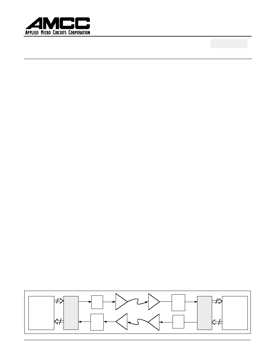
dards. Figure 1, shows a typical network application.
The other application block diagrams are shown in
Figures 2, 3 and 4.
On-chip clock synthesis PLL components are con-
tained in the S19237 chip, allowing the use of a slower
external transmit clock reference. The chip can be
used with 155.52 MHz or 622.08 MHz (or equivalent
FEC/10 GB Ethernet rate) reference clocks, in support
of existing system clocking schemes. The low-jitter
LVDS interface guarantees compliance with the bit-
error rate requirements of the Telecordia and ITU-T
standards. The S19237 is packaged in a 255 PBGA
package, offering designers a small package outline.
Figure 1. System Block Diagram
ORX
OTX
ORX
OTX
AMCC
S19237
16
AMCC'S
KHATANGA,
GANGES,
HUDSON,
MEKONG,
or RUBICON
AMCC
S3390
TIA
Laser
Driver
Laser
Driver
AMCC
S19237
AMCC
S3390
TIA
16
AMCC'S
KHATANGA,
GANGES,
HUDSON,
MEKONG,
or RUBICON
相關(guān)PDF資料 |
PDF描述 |
|---|---|
| S1950E-FREQ-OUT25 | CRYSTAL OSCILLATOR, CLOCK, 80 MHz - 125 MHz, ACMOS OUTPUT |
| S1F78100Y2A0 | 6 V FIXED POSITIVE REGULATOR, PSSO3 |
| S1F78100Y2B0 | 5 V FIXED POSITIVE REGULATOR, PSSO3 |
| S1F78100Y2C0 | 3.2 V FIXED POSITIVE REGULATOR, PSSO3 |
| S1F78100Y2F0 | 2.2 V FIXED POSITIVE REGULATOR, PSSO3 |
相關(guān)代理商/技術(shù)參數(shù) |
參數(shù)描述 |
|---|---|
| S19237PB13-2 | 制造商:AppliedMicro 功能描述: |
| S19237PBICC | 制造商:AppliedMicro 功能描述:IC INTERFACE TRANSCEIVER LOW POWER CMOS 255 BGA 制造商:AMCC 功能描述: |
| S19238CBI | 制造商:AppliedMicro 功能描述: |
| S19250 | 制造商:AMCC 制造商全稱:Applied Micro Circuits Corporation 功能描述:STS-192 SONET/SDH/FEC/GbE/FC 16-bit Transceiver with EDC |
| S19250PBIC | 制造商:AppliedMicro 功能描述:10G SERDES EDC/SFI-4 |
發(fā)布緊急采購(gòu),3分鐘左右您將得到回復(fù)。