- 您現(xiàn)在的位置:買賣IC網(wǎng) > PDF目錄67723 > IXF1010 (INTEL CORP) 10 CHANNEL(S), 1000M bps, LOCAL AREA NETWORK CONTROLLER, CBGA552 PDF資料下載
參數(shù)資料
| 型號(hào): | IXF1010 |
| 廠商: | INTEL CORP |
| 元件分類: | 微控制器/微處理器 |
| 英文描述: | 10 CHANNEL(S), 1000M bps, LOCAL AREA NETWORK CONTROLLER, CBGA552 |
| 封裝: | 25 X 25 MM, 1 MM PITCH, CERAMIC, BGA-552 |
| 文件頁(yè)數(shù): | 54/116頁(yè) |
| 文件大小: | 1392K |
| 代理商: | IXF1010 |
第1頁(yè)第2頁(yè)第3頁(yè)第4頁(yè)第5頁(yè)第6頁(yè)第7頁(yè)第8頁(yè)第9頁(yè)第10頁(yè)第11頁(yè)第12頁(yè)第13頁(yè)第14頁(yè)第15頁(yè)第16頁(yè)第17頁(yè)第18頁(yè)第19頁(yè)第20頁(yè)第21頁(yè)第22頁(yè)第23頁(yè)第24頁(yè)第25頁(yè)第26頁(yè)第27頁(yè)第28頁(yè)第29頁(yè)第30頁(yè)第31頁(yè)第32頁(yè)第33頁(yè)第34頁(yè)第35頁(yè)第36頁(yè)第37頁(yè)第38頁(yè)第39頁(yè)第40頁(yè)第41頁(yè)第42頁(yè)第43頁(yè)第44頁(yè)第45頁(yè)第46頁(yè)第47頁(yè)第48頁(yè)第49頁(yè)第50頁(yè)第51頁(yè)第52頁(yè)第53頁(yè)當(dāng)前第54頁(yè)第55頁(yè)第56頁(yè)第57頁(yè)第58頁(yè)第59頁(yè)第60頁(yè)第61頁(yè)第62頁(yè)第63頁(yè)第64頁(yè)第65頁(yè)第66頁(yè)第67頁(yè)第68頁(yè)第69頁(yè)第70頁(yè)第71頁(yè)第72頁(yè)第73頁(yè)第74頁(yè)第75頁(yè)第76頁(yè)第77頁(yè)第78頁(yè)第79頁(yè)第80頁(yè)第81頁(yè)第82頁(yè)第83頁(yè)第84頁(yè)第85頁(yè)第86頁(yè)第87頁(yè)第88頁(yè)第89頁(yè)第90頁(yè)第91頁(yè)第92頁(yè)第93頁(yè)第94頁(yè)第95頁(yè)第96頁(yè)第97頁(yè)第98頁(yè)第99頁(yè)第100頁(yè)第101頁(yè)第102頁(yè)第103頁(yè)第104頁(yè)第105頁(yè)第106頁(yè)第107頁(yè)第108頁(yè)第109頁(yè)第110頁(yè)第111頁(yè)第112頁(yè)第113頁(yè)第114頁(yè)第115頁(yè)第116頁(yè)
IXF1010 — 10-Port 100/1000 Mbps Ethernet MAC
42
Preliminary Datasheet
Document #: 249839
Revision #: 001
Rev. Date: April 29, 2002
Mode 1: (LED_SEL_MODE = 1): This mode is used with standard TTL (74LS595) or HCMOS
(74HC595) octal shift registers with latches, providing the most general and cost-effective
implementation of the serial data stream conversion.
In addition to these physical modes of operation, there are two types of specific LED data decodes
available. This option is a global selection and controls the operation of all ports (see Table 68,
3.5.3
LED Interface Signal Description
The IXF1010 LED Interface consists of three output signal pins that are 2.5V CMOS level pads.
Table 11 provides LED signal names, pin numbers, and descriptions.
3.5.4
Mode 0: Detailed Operation
Note:
Please refer to the SGS Thompson M5450 datasheet for device-operation information.
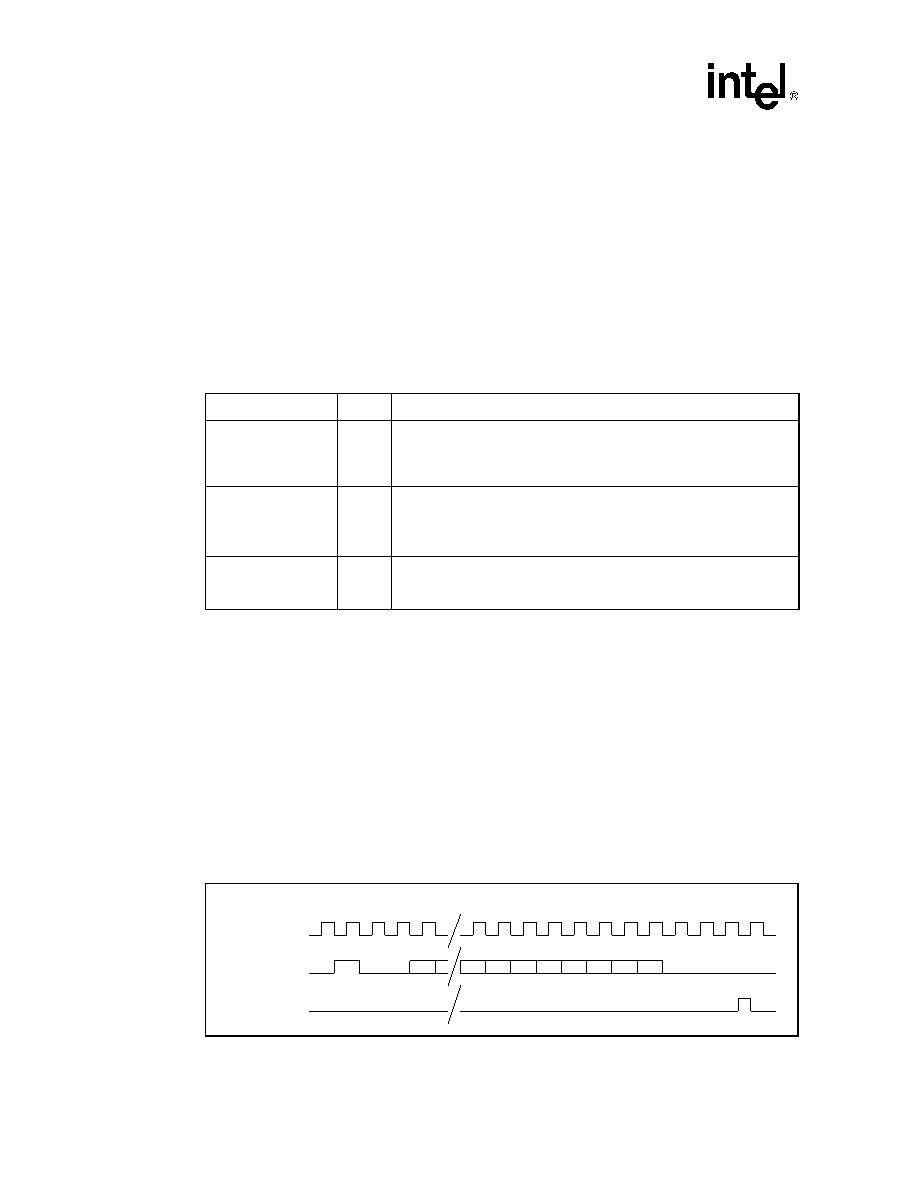
The operation of the LED Interface in Mode 0 is based on a 36-bit counter loop. The data for each
LED is placed in turn on the serial data line and clocked out by the LED_CLK. Figure 15 on
page 42 shows the basic timing relationship and relative positioning in the data stream of each bit.
Figure 15 shows the 36 clocks that are output on the LED_CLK pin. The data changes on the
falling edge of the clock and is valid for almost the entire clock cycle. This ensures that the data is
valid during the rising edge of the LED_CLK, which is used to clock the data into the M5450
device.The actual data shown in Figure 15 consists of a chain of 36 bits only, 30 of which are valid
LED DATA. The 36-bit data chain is built up as follows:
Table 11. LED Pin Descriptions
Pin Name
Pin #
Pin Description
LED_CLK
A20
LED_CLK: This signal is an output that provides a continuous clock
synchronous to the serial data stream output on the LED_DATA pin. This
clock has a maximum speed of 0.5 MHz
The behavior of this signal remains constant in all modes of operation.
LED_DATA
A19
LED_DATA: This signal provides the data, in various formats, as a serial bit
stream. The data must be valid on the rising edge of the LED_CLK signal.
In Mode 0, the data presented on this pin is TRUE (Logic 1 = High).
In Mode 1, the data presented on this pin is INVERTED (Logic 1 = Low).
LED_LATCH
K18
LED_LATCH: This is an output pin and the signal is used only in Mode 1 as
the Latch enable for the shift register chain.
This signal is not used in Mode 0, and should be left unconnected.
Figure 15. Mode 0 Timing Diagram
1
23 24 25 26 27 28 29 30
135
26
23
4
LED_CLK
LED_DATA
LED_LATCH
34
27
33
32
31
30
29
28
36
相關(guān)PDF資料 |
PDF描述 |
|---|---|
| JANTX1N3595US-1 | 0.15 A, SILICON, SIGNAL DIODE |
| JAN1N3595US-1 | 0.15 A, SILICON, SIGNAL DIODE |
| JANTXV1N3595US-1 | 0.15 A, SILICON, SIGNAL DIODE |
| JANS1N3595-1 | 0.15 A, 125 V, SILICON, SIGNAL DIODE, DO-35 |
| JAN1N3595 | 0.15 A, SILICON, SIGNAL DIODE, DO-35 |
相關(guān)代理商/技術(shù)參數(shù) |
參數(shù)描述 |
|---|---|
| IXF102A | 功能描述:IRIX II GREY HEADLAMP 5LED FLOOD RoHS:是 類別:工具 >> 閃光燈 系列:Irix™ II 標(biāo)準(zhǔn)包裝:1 系列:- 類型:筆形手電筒 燈類型:LED 燈輸出:- 特點(diǎn):可變強(qiáng)度 電池大小:AA(需要 1 個(gè)) 長(zhǎng)度:- 主體材料:- |
| IXF-10A15AF | 制造商:ILSI 制造商全稱:ILSI America LLC 功能描述:Crystal Filter 3 Lead Metal Package |
| IXF-10A15AT | 制造商:ILSI 制造商全稱:ILSI America LLC 功能描述:Crystal Filter 3 Lead Metal Package |
| IXF-10A15BF | 制造商:ILSI 制造商全稱:ILSI America LLC 功能描述:Crystal Filter 3 Lead Metal Package |
| IXF-10A15BT | 制造商:ILSI 制造商全稱:ILSI America LLC 功能描述:Crystal Filter 3 Lead Metal Package |
發(fā)布緊急采購(gòu),3分鐘左右您將得到回復(fù)。