- 您現(xiàn)在的位置:買賣IC網(wǎng) > PDF目錄98007 > M44C510-P40 (ATMEL CORP) 4-BIT, MROM, MICROCONTROLLER, PDIP40 PDF資料下載
參數(shù)資料
| 型號: | M44C510-P40 |
| 廠商: | ATMEL CORP |
| 元件分類: | 微控制器/微處理器 |
| 英文描述: | 4-BIT, MROM, MICROCONTROLLER, PDIP40 |
| 封裝: | DIP-40 |
| 文件頁數(shù): | 13/57頁 |
| 文件大小: | 1105K |
| 代理商: | M44C510-P40 |
第1頁第2頁第3頁第4頁第5頁第6頁第7頁第8頁第9頁第10頁第11頁第12頁當(dāng)前第13頁第14頁第15頁第16頁第17頁第18頁第19頁第20頁第21頁第22頁第23頁第24頁第25頁第26頁第27頁第28頁第29頁第30頁第31頁第32頁第33頁第34頁第35頁第36頁第37頁第38頁第39頁第40頁第41頁第42頁第43頁第44頁第45頁第46頁第47頁第48頁第49頁第50頁第51頁第52頁第53頁第54頁第55頁第56頁第57頁
M44C510
TELEFUNKEN Semiconductors
Rev. A2, 13-Jan-98
20 (57)
2.2.4
Bidirectional Port 6
Master reset
Q
V
DD
V
DD
BP6y
Mask options
*
P6DATy
I/O Bus
D
IN enable
I/O Bus
*
Pull-up
Pull-down
V
DD
*
Static
Pull-up
(Data out)
*
S
96 11525
y = 0 or 1
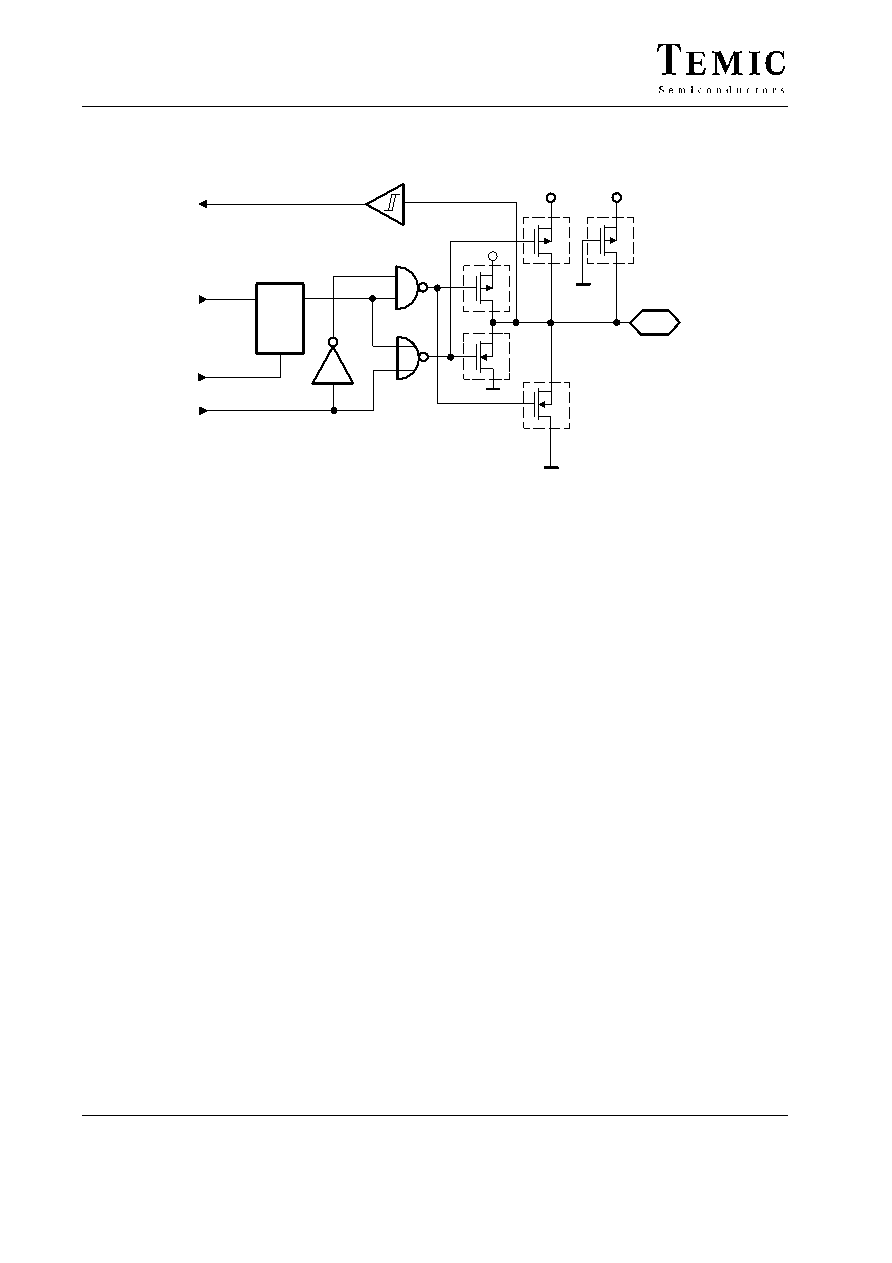
Figure 16. Bidirectional Port 6
This 2-bit bidirectional port can be used as bitwise-pro-
grammable I/O. The data is LSB aligned so that the two
MSB’s will not appear on the port pins when written. The
port pins can also be used as external interrupt inputs (see
figures 15 and 16). Both interrupts can be masked or inde-
pendently configured to trigger on either edge. The
interrupt priority levels are also configurable. The
interrupt configuration and port direction is controlled by
the Port 6 Control Register (P6CR). An additional low
resistance pull-up transistor (mask option) provides an
internal bus pull-up for serial bus applications.
In output mode (PxDDR bit = 0), the respective Port Data
Register (PxDAT) bit appears on the port pin, driven by
an output port driver stage which can be mask pro-
grammed as open drain, or full complementary CMOS.
With an IN instruction the actual pin state can be read
back into the controller at any time without changing the
port directional mode. If the output port is mask config-
ured as an open drain driver, the controller is able to
receive the external data on this pin without switching
into input mode as long as the output transistor is switched
off.
In input mode (PxDDR bit = 1), the output driver stage is
deactivated, so that an IN instruction will directly read the
pin state which can be driven from an external source. In
this case, the state of the Port Data Register (PxDAT),
although not appearing at the pin itself, remains
unchanged. High resistance mask selectable pull-up or
pull-down transistors are automatically switched onto the
port pin in input mode. The Port Data Register is written
to the respective port address with an OUT instruction.
The Port 6 Data Register (P6DAT) is I/O mapped to the
primary address register of address ’6’hex and the Port 6
Control Register (P6CR) to the corresponding auxiliary
register. The P6CR is a byte wide register and is written
by writing the low nibble first and then the high nibble
(see section 2.1 “Addressing peripherals”).
相關(guān)PDF資料 |
PDF描述 |
|---|---|
| M44C510D-XXX-DOW | 4-BIT, MROM, MICROCONTROLLER |
| M44C588 | 4-BIT, MROM, 4 MHz, MICROCONTROLLER |
| M44C892 | 4-BIT, MROM, 4 MHz, MICROCONTROLLER, PDSO20 |
| M48T08Y-15PC1 | 0 TIMER(S), REAL TIME CLOCK, PDMA28 |
| M48T08Y-10PC1 | 0 TIMER(S), REAL TIME CLOCK, PDMA28 |
相關(guān)代理商/技術(shù)參數(shù) |
參數(shù)描述 |
|---|---|
| M44C890 | 制造商:ATMEL 制造商全稱:ATMEL Corporation 功能描述:Low-Current Microcontroller for Wireless Communication |
| M44C890-H | 制造商:ATMEL 制造商全稱:ATMEL Corporation 功能描述:Low-Current Microcontroller for Wireless Communication |
| M44S05K4F1 | 功能描述:汽車連接器 MX44 Terminals RoHS:否 制造商:Amphenol SINE Systems 產(chǎn)品:Contacts 系列:ATP 位置數(shù)量: 型式:Female 安裝風(fēng)格: 端接類型: 觸點(diǎn)電鍍:Nickel |
| M44T332538880MHZ | 制造商:MEC 功能描述: |
| M44T3338880MHZ | 制造商:MEC 功能描述: |
發(fā)布緊急采購,3分鐘左右您將得到回復(fù)。