- 您現(xiàn)在的位置:買賣IC網(wǎng) > PDF目錄370837 > M32C (Mitsubishi Electric Corporation) SINGLE-CHIP 16-BIT CMOS MICROCOMPUTER PDF資料下載
參數(shù)資料
| 型號: | M32C |
| 廠商: | Mitsubishi Electric Corporation |
| 英文描述: | SINGLE-CHIP 16-BIT CMOS MICROCOMPUTER |
| 中文描述: | 單片16位CMOS微機 |
| 文件頁數(shù): | 433/441頁 |
| 文件大小: | 5170K |
| 代理商: | M32C |
第1頁第2頁第3頁第4頁第5頁第6頁第7頁第8頁第9頁第10頁第11頁第12頁第13頁第14頁第15頁第16頁第17頁第18頁第19頁第20頁第21頁第22頁第23頁第24頁第25頁第26頁第27頁第28頁第29頁第30頁第31頁第32頁第33頁第34頁第35頁第36頁第37頁第38頁第39頁第40頁第41頁第42頁第43頁第44頁第45頁第46頁第47頁第48頁第49頁第50頁第51頁第52頁第53頁第54頁第55頁第56頁第57頁第58頁第59頁第60頁第61頁第62頁第63頁第64頁第65頁第66頁第67頁第68頁第69頁第70頁第71頁第72頁第73頁第74頁第75頁第76頁第77頁第78頁第79頁第80頁第81頁第82頁第83頁第84頁第85頁第86頁第87頁第88頁第89頁第90頁第91頁第92頁第93頁第94頁第95頁第96頁第97頁第98頁第99頁第100頁第101頁第102頁第103頁第104頁第105頁第106頁第107頁第108頁第109頁第110頁第111頁第112頁第113頁第114頁第115頁第116頁第117頁第118頁第119頁第120頁第121頁第122頁第123頁第124頁第125頁第126頁第127頁第128頁第129頁第130頁第131頁第132頁第133頁第134頁第135頁第136頁第137頁第138頁第139頁第140頁第141頁第142頁第143頁第144頁第145頁第146頁第147頁第148頁第149頁第150頁第151頁第152頁第153頁第154頁第155頁第156頁第157頁第158頁第159頁第160頁第161頁第162頁第163頁第164頁第165頁第166頁第167頁第168頁第169頁第170頁第171頁第172頁第173頁第174頁第175頁第176頁第177頁第178頁第179頁第180頁第181頁第182頁第183頁第184頁第185頁第186頁第187頁第188頁第189頁第190頁第191頁第192頁第193頁第194頁第195頁第196頁第197頁第198頁第199頁第200頁第201頁第202頁第203頁第204頁第205頁第206頁第207頁第208頁第209頁第210頁第211頁第212頁第213頁第214頁第215頁第216頁第217頁第218頁第219頁第220頁第221頁第222頁第223頁第224頁第225頁第226頁第227頁第228頁第229頁第230頁第231頁第232頁第233頁第234頁第235頁第236頁第237頁第238頁第239頁第240頁第241頁第242頁第243頁第244頁第245頁第246頁第247頁第248頁第249頁第250頁第251頁第252頁第253頁第254頁第255頁第256頁第257頁第258頁第259頁第260頁第261頁第262頁第263頁第264頁第265頁第266頁第267頁第268頁第269頁第270頁第271頁第272頁第273頁第274頁第275頁第276頁第277頁第278頁第279頁第280頁第281頁第282頁第283頁第284頁第285頁第286頁第287頁第288頁第289頁第290頁第291頁第292頁第293頁第294頁第295頁第296頁第297頁第298頁第299頁第300頁第301頁第302頁第303頁第304頁第305頁第306頁第307頁第308頁第309頁第310頁第311頁第312頁第313頁第314頁第315頁第316頁第317頁第318頁第319頁第320頁第321頁第322頁第323頁第324頁第325頁第326頁第327頁第328頁第329頁第330頁第331頁第332頁第333頁第334頁第335頁第336頁第337頁第338頁第339頁第340頁第341頁第342頁第343頁第344頁第345頁第346頁第347頁第348頁第349頁第350頁第351頁第352頁第353頁第354頁第355頁第356頁第357頁第358頁第359頁第360頁第361頁第362頁第363頁第364頁第365頁第366頁第367頁第368頁第369頁第370頁第371頁第372頁第373頁第374頁第375頁第376頁第377頁第378頁第379頁第380頁第381頁第382頁第383頁第384頁第385頁第386頁第387頁第388頁第389頁第390頁第391頁第392頁第393頁第394頁第395頁第396頁第397頁第398頁第399頁第400頁第401頁第402頁第403頁第404頁第405頁第406頁第407頁第408頁第409頁第410頁第411頁第412頁第413頁第414頁第415頁第416頁第417頁第418頁第419頁第420頁第421頁第422頁第423頁第424頁第425頁第426頁第427頁第428頁第429頁第430頁第431頁第432頁當前第433頁第434頁第435頁第436頁第437頁第438頁第439頁第440頁第441頁
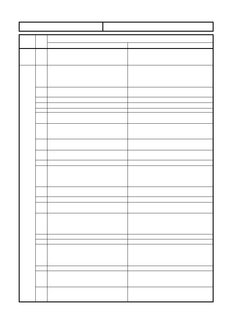
REVISION HISTORY
M32C/83 GROUP DATA SHEET
Rev.
Date
Description
Page
Errror
Correct
( 1 / 7 )
B1
1/8/2001
100-pin version is added.
Flash memory version is added.
Others
2,3
Tables 1.1.1 and 1.1.2
Interrupt: 12 internal/external sources
(intelligent I/O and CAN module)
Supply voltage
A-D converter
10 bits (8 channels) x 2 circuits, max 26 inputs
Table 1.1.3
Pin 26
10-12 Figures 1.1.4, 1.1.5, Table 1.1.7
11
Figure 1.1.5 Pin 97 AN0
0
12
Pin 32 (FP)
Vcc
Pin 34 (FP)
Vss
13
Vcc position to pin 64(FP)
Vss position to pin 66(FP)
RxD4/SCL4/STxD4 position to pin 98 (FP)
14
Table 1.1.5
AN2
0
to AN2
7
AN3
0
to AN3
7
17
Table1.1.12
P12
0
to P12
7
ISCLK description
AN1
0
to AN1
7
18
Figure 1.1.6 System clock oscillation circuit
28, 29 Figure 1.4.3 (122), (167)
Delate
3.0 to 3.6V (f(X
IN
)=20MHz without wait) add
3
10 bits x 2 circuits, standard 10 inputs, max 26 inputs
CAN
IN
addition
CAN
IN
is added to Pin 17(GP) and pin 19(FP)
AN
0
Delate
Delate
Pin 62
Pin 64
Pin 100
AN0
0
to AN0
7
AN2
0
to AN2
7
Delate
AN15
0
to AN15
7
PLL oscillation stop detect addition
Group0 receive buffer register, Group1 receive buffer
register
Group0 transmit buffer/receive data register, Group1
transmit buffer/receive data register
Addresses 03A0
16
, 03A1
16
, 03B9
16
, 03BC
16
, 03BD
16
,
03C9
16
, 03CB
16
to 03D3
16
Addition. Displase after the former Note 2
7
(123), (168)
46
Note 1: Addresses 03C9
16
, 03CB
16
to 03D3
16
48
70
Figure 1.6.1 Note 2
Figure 1.8.6
When reset of PLL control register 0
0X11 0100
Figure 1.8.8 Count value set bit
Count start bit
Count stop/start
Note 2
Line 10
Addition
Line 8
1:Sub clock is selected
Figure 1.14.2 Values that can be set Pulse width
modulation mode (8-bit PWM)
00
16
to FF
16
(High-order and low-order address)
0011 0100
Division rate select bit
Operation enable bit
Divider stops/starts
Delate
Stop mode is canceled before setting this bit to "1".
1: Clock from ring oscillator is selected
72
76
77
135
00
16
to FE
16
(High-order address) 00
16
to FF
16
(Low-
order address)
TrmData
230
266
Line 5, Bit 1
Table1.23.11 Waveform generate control register
1when clock synchronous serial I/O
-
Table1.23.17 Note 1:
TrmActive
√
When the transfer clock and transfer data are trans-
mission, transfer clock is set to at least 6 divisions of
280
B1
30/8/
2001
相關PDF資料 |
PDF描述 |
|---|---|
| M34225M2-XXXSP | SINGLE-CHIP 4-BIT CMOS MICRCOMPUTERl |
| M34225M1 | SINGLE-CHIP 4-BIT CMOS MICRCOMPUTERl |
| M34225M1-XXXFP | SINGLE-CHIP 4-BIT CMOS MICRCOMPUTERl |
| M34225M1-XXXSP | SINGLE-CHIP 4-BIT CMOS MICRCOMPUTERl |
| M34225M2-XXXFP | SINGLE-CHIP 4-BIT CMOS MICRCOMPUTERl |
相關代理商/技術參數(shù) |
參數(shù)描述 |
|---|---|
| M32C/83 | 制造商:MITSUBISHI 制造商全稱:Mitsubishi Electric Semiconductor 功能描述:SINGLE-CHIP 16-BIT CMOS MICROCOMPUTER |
| M32C/86 | 制造商:RENESAS 制造商全稱:Renesas Technology Corp 功能描述:RENESAS 16/32-BIT SINGLE-CHIP MICROCOMPUTER M16C FAMILY / M32C/80 SERIES |
| M32C/86T | 制造商:RENESAS 制造商全稱:Renesas Technology Corp 功能描述:RENESAS 16/32-BIT SINGLE-CHIP MICROCOMPUTER M16C FAMILY / M32C/80 SERIES |
| M32C/8A | 制造商:RENESAS 制造商全稱:Renesas Technology Corp 功能描述:RENESAS MCU M16C FAMILY / M32C/80 Series |
| M32C/8B | 制造商:RENESAS 制造商全稱:Renesas Technology Corp 功能描述:RENESAS MCU M16C FAMILY / M32C/80 SERIES |
發(fā)布緊急采購,3分鐘左右您將得到回復。