- 您現(xiàn)在的位置:買賣IC網(wǎng) > PDF目錄370837 > M32C (Mitsubishi Electric Corporation) SINGLE-CHIP 16-BIT CMOS MICROCOMPUTER PDF資料下載
參數(shù)資料
| 型號(hào): | M32C |
| 廠商: | Mitsubishi Electric Corporation |
| 英文描述: | SINGLE-CHIP 16-BIT CMOS MICROCOMPUTER |
| 中文描述: | 單片16位CMOS微機(jī) |
| 文件頁(yè)數(shù): | 16/441頁(yè) |
| 文件大小: | 5170K |
| 代理商: | M32C |
第1頁(yè)第2頁(yè)第3頁(yè)第4頁(yè)第5頁(yè)第6頁(yè)第7頁(yè)第8頁(yè)第9頁(yè)第10頁(yè)第11頁(yè)第12頁(yè)第13頁(yè)第14頁(yè)第15頁(yè)當(dāng)前第16頁(yè)第17頁(yè)第18頁(yè)第19頁(yè)第20頁(yè)第21頁(yè)第22頁(yè)第23頁(yè)第24頁(yè)第25頁(yè)第26頁(yè)第27頁(yè)第28頁(yè)第29頁(yè)第30頁(yè)第31頁(yè)第32頁(yè)第33頁(yè)第34頁(yè)第35頁(yè)第36頁(yè)第37頁(yè)第38頁(yè)第39頁(yè)第40頁(yè)第41頁(yè)第42頁(yè)第43頁(yè)第44頁(yè)第45頁(yè)第46頁(yè)第47頁(yè)第48頁(yè)第49頁(yè)第50頁(yè)第51頁(yè)第52頁(yè)第53頁(yè)第54頁(yè)第55頁(yè)第56頁(yè)第57頁(yè)第58頁(yè)第59頁(yè)第60頁(yè)第61頁(yè)第62頁(yè)第63頁(yè)第64頁(yè)第65頁(yè)第66頁(yè)第67頁(yè)第68頁(yè)第69頁(yè)第70頁(yè)第71頁(yè)第72頁(yè)第73頁(yè)第74頁(yè)第75頁(yè)第76頁(yè)第77頁(yè)第78頁(yè)第79頁(yè)第80頁(yè)第81頁(yè)第82頁(yè)第83頁(yè)第84頁(yè)第85頁(yè)第86頁(yè)第87頁(yè)第88頁(yè)第89頁(yè)第90頁(yè)第91頁(yè)第92頁(yè)第93頁(yè)第94頁(yè)第95頁(yè)第96頁(yè)第97頁(yè)第98頁(yè)第99頁(yè)第100頁(yè)第101頁(yè)第102頁(yè)第103頁(yè)第104頁(yè)第105頁(yè)第106頁(yè)第107頁(yè)第108頁(yè)第109頁(yè)第110頁(yè)第111頁(yè)第112頁(yè)第113頁(yè)第114頁(yè)第115頁(yè)第116頁(yè)第117頁(yè)第118頁(yè)第119頁(yè)第120頁(yè)第121頁(yè)第122頁(yè)第123頁(yè)第124頁(yè)第125頁(yè)第126頁(yè)第127頁(yè)第128頁(yè)第129頁(yè)第130頁(yè)第131頁(yè)第132頁(yè)第133頁(yè)第134頁(yè)第135頁(yè)第136頁(yè)第137頁(yè)第138頁(yè)第139頁(yè)第140頁(yè)第141頁(yè)第142頁(yè)第143頁(yè)第144頁(yè)第145頁(yè)第146頁(yè)第147頁(yè)第148頁(yè)第149頁(yè)第150頁(yè)第151頁(yè)第152頁(yè)第153頁(yè)第154頁(yè)第155頁(yè)第156頁(yè)第157頁(yè)第158頁(yè)第159頁(yè)第160頁(yè)第161頁(yè)第162頁(yè)第163頁(yè)第164頁(yè)第165頁(yè)第166頁(yè)第167頁(yè)第168頁(yè)第169頁(yè)第170頁(yè)第171頁(yè)第172頁(yè)第173頁(yè)第174頁(yè)第175頁(yè)第176頁(yè)第177頁(yè)第178頁(yè)第179頁(yè)第180頁(yè)第181頁(yè)第182頁(yè)第183頁(yè)第184頁(yè)第185頁(yè)第186頁(yè)第187頁(yè)第188頁(yè)第189頁(yè)第190頁(yè)第191頁(yè)第192頁(yè)第193頁(yè)第194頁(yè)第195頁(yè)第196頁(yè)第197頁(yè)第198頁(yè)第199頁(yè)第200頁(yè)第201頁(yè)第202頁(yè)第203頁(yè)第204頁(yè)第205頁(yè)第206頁(yè)第207頁(yè)第208頁(yè)第209頁(yè)第210頁(yè)第211頁(yè)第212頁(yè)第213頁(yè)第214頁(yè)第215頁(yè)第216頁(yè)第217頁(yè)第218頁(yè)第219頁(yè)第220頁(yè)第221頁(yè)第222頁(yè)第223頁(yè)第224頁(yè)第225頁(yè)第226頁(yè)第227頁(yè)第228頁(yè)第229頁(yè)第230頁(yè)第231頁(yè)第232頁(yè)第233頁(yè)第234頁(yè)第235頁(yè)第236頁(yè)第237頁(yè)第238頁(yè)第239頁(yè)第240頁(yè)第241頁(yè)第242頁(yè)第243頁(yè)第244頁(yè)第245頁(yè)第246頁(yè)第247頁(yè)第248頁(yè)第249頁(yè)第250頁(yè)第251頁(yè)第252頁(yè)第253頁(yè)第254頁(yè)第255頁(yè)第256頁(yè)第257頁(yè)第258頁(yè)第259頁(yè)第260頁(yè)第261頁(yè)第262頁(yè)第263頁(yè)第264頁(yè)第265頁(yè)第266頁(yè)第267頁(yè)第268頁(yè)第269頁(yè)第270頁(yè)第271頁(yè)第272頁(yè)第273頁(yè)第274頁(yè)第275頁(yè)第276頁(yè)第277頁(yè)第278頁(yè)第279頁(yè)第280頁(yè)第281頁(yè)第282頁(yè)第283頁(yè)第284頁(yè)第285頁(yè)第286頁(yè)第287頁(yè)第288頁(yè)第289頁(yè)第290頁(yè)第291頁(yè)第292頁(yè)第293頁(yè)第294頁(yè)第295頁(yè)第296頁(yè)第297頁(yè)第298頁(yè)第299頁(yè)第300頁(yè)第301頁(yè)第302頁(yè)第303頁(yè)第304頁(yè)第305頁(yè)第306頁(yè)第307頁(yè)第308頁(yè)第309頁(yè)第310頁(yè)第311頁(yè)第312頁(yè)第313頁(yè)第314頁(yè)第315頁(yè)第316頁(yè)第317頁(yè)第318頁(yè)第319頁(yè)第320頁(yè)第321頁(yè)第322頁(yè)第323頁(yè)第324頁(yè)第325頁(yè)第326頁(yè)第327頁(yè)第328頁(yè)第329頁(yè)第330頁(yè)第331頁(yè)第332頁(yè)第333頁(yè)第334頁(yè)第335頁(yè)第336頁(yè)第337頁(yè)第338頁(yè)第339頁(yè)第340頁(yè)第341頁(yè)第342頁(yè)第343頁(yè)第344頁(yè)第345頁(yè)第346頁(yè)第347頁(yè)第348頁(yè)第349頁(yè)第350頁(yè)第351頁(yè)第352頁(yè)第353頁(yè)第354頁(yè)第355頁(yè)第356頁(yè)第357頁(yè)第358頁(yè)第359頁(yè)第360頁(yè)第361頁(yè)第362頁(yè)第363頁(yè)第364頁(yè)第365頁(yè)第366頁(yè)第367頁(yè)第368頁(yè)第369頁(yè)第370頁(yè)第371頁(yè)第372頁(yè)第373頁(yè)第374頁(yè)第375頁(yè)第376頁(yè)第377頁(yè)第378頁(yè)第379頁(yè)第380頁(yè)第381頁(yè)第382頁(yè)第383頁(yè)第384頁(yè)第385頁(yè)第386頁(yè)第387頁(yè)第388頁(yè)第389頁(yè)第390頁(yè)第391頁(yè)第392頁(yè)第393頁(yè)第394頁(yè)第395頁(yè)第396頁(yè)第397頁(yè)第398頁(yè)第399頁(yè)第400頁(yè)第401頁(yè)第402頁(yè)第403頁(yè)第404頁(yè)第405頁(yè)第406頁(yè)第407頁(yè)第408頁(yè)第409頁(yè)第410頁(yè)第411頁(yè)第412頁(yè)第413頁(yè)第414頁(yè)第415頁(yè)第416頁(yè)第417頁(yè)第418頁(yè)第419頁(yè)第420頁(yè)第421頁(yè)第422頁(yè)第423頁(yè)第424頁(yè)第425頁(yè)第426頁(yè)第427頁(yè)第428頁(yè)第429頁(yè)第430頁(yè)第431頁(yè)第432頁(yè)第433頁(yè)第434頁(yè)第435頁(yè)第436頁(yè)第437頁(yè)第438頁(yè)第439頁(yè)第440頁(yè)第441頁(yè)
deveopmen
Description
Rev.B2 for proof reading
Mitsubishi Microcomputers
M32C/83 group
SINGLE-CHIP 16-BIT CMOS MICROCOMPUTER
16
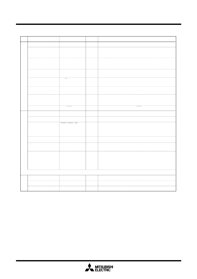
Table 1.1.11. Pin description (3/4)
Function
I/O port
Sub clock input
UART port
Description
I/O
I
O
I/O
I/O
I/O
I/O
I
I/O type
P8
0
-P8
4
, P8
6
, P8
7
X
CIN
INPC/ISRxD/BE
IN
Pin name
P8
P9
Port
I/O port
Intelligent I/O port
P9
0
to P9
7
This is a 7-bit I/O port equivalent to P0.
P8
6
and P8
7
function as I/O ports for the sub clock
generating circuit by software. Connect a crystal between
the X
CIN
and the X
COUT
pins.
When using PLL frequency synthesizer, connect P8
7
to a
low-pass filter. To stabilize PLL frequency, connect P8
6
to
Vss.
P9
0
to P9
3
are I/O ports for UART3.
P9
4
to P9
7
are I/O ports for UART4.
I
This is an 8-bit I/O port equivalent to P0.
I/O
INPC is an input port for time measurement function.
ISRxD/BE
IN
is receive data input port for intelligent I/O
communication.
Input port and input ports for NMI interrupt.
CTS/RTS/SS
CLK
RxD/SCL/STxD
TxD/SDA/SRxD
DA0, DA1
Timer A port
Three phase motor
control output port
External interrupt input
port
P8
0
to P8
1
are I/O ports for timer A4.
P8
0
and P8
1
are U phase output ports.
O
I
TA4
OUT
TA4
IN
P8
2
to P8
4
are external interrupt input ports.
I
INT
0
to INT
2
Input port
P8
5
/NMI
I
TB0
IN
to TB4
IN
Timer B port
P9
0
to P9
4
are input port for timer B4.
O
D-A output port
P9
3
and P9
4
are D-A output ports.
I
I
ANEX1, ANEX2
AD
TRG
OUTC/IE
OUT
A-D related port
P9
5
to P9
6
are expanded input port for A-D converter.
P9
7
is A-D trigger input port.
OUTC is an output port for waveform generation function.
IE
OUT
is transmit data output port for intelligent I/O
communication.
IE
IN
is receive data input port for intelligent I/O
communication.
Intelligent I/O port
IE
IN
Key input interrupt port
I
I/O
I
KI
0
to KI
3
AN
0
to AN
7
P10
I/O port
Analog input port
P10
0
to P10
7
This is an 8-bit I/O port equivalent to P0.
P10
4
to P10
7
are key input interrupt ports.
P10
0
to P10
7
are analog input ports for A-D convertor.
The protect register prevents a false write to P9 direction register and function select register A3.
U, U
I/O
I
X
COUT
O
Sub clock output
V
COUT
O
Low-pass filter connect
pin for PLL frequency
synthesizer
相關(guān)PDF資料 |
PDF描述 |
|---|---|
| M34225M2-XXXSP | SINGLE-CHIP 4-BIT CMOS MICRCOMPUTERl |
| M34225M1 | SINGLE-CHIP 4-BIT CMOS MICRCOMPUTERl |
| M34225M1-XXXFP | SINGLE-CHIP 4-BIT CMOS MICRCOMPUTERl |
| M34225M1-XXXSP | SINGLE-CHIP 4-BIT CMOS MICRCOMPUTERl |
| M34225M2-XXXFP | SINGLE-CHIP 4-BIT CMOS MICRCOMPUTERl |
相關(guān)代理商/技術(shù)參數(shù) |
參數(shù)描述 |
|---|---|
| M32C/83 | 制造商:MITSUBISHI 制造商全稱:Mitsubishi Electric Semiconductor 功能描述:SINGLE-CHIP 16-BIT CMOS MICROCOMPUTER |
| M32C/86 | 制造商:RENESAS 制造商全稱:Renesas Technology Corp 功能描述:RENESAS 16/32-BIT SINGLE-CHIP MICROCOMPUTER M16C FAMILY / M32C/80 SERIES |
| M32C/86T | 制造商:RENESAS 制造商全稱:Renesas Technology Corp 功能描述:RENESAS 16/32-BIT SINGLE-CHIP MICROCOMPUTER M16C FAMILY / M32C/80 SERIES |
| M32C/8A | 制造商:RENESAS 制造商全稱:Renesas Technology Corp 功能描述:RENESAS MCU M16C FAMILY / M32C/80 Series |
| M32C/8B | 制造商:RENESAS 制造商全稱:Renesas Technology Corp 功能描述:RENESAS MCU M16C FAMILY / M32C/80 SERIES |
發(fā)布緊急采購(gòu),3分鐘左右您將得到回復(fù)。