- 您現(xiàn)在的位置:買賣IC網(wǎng) > PDF目錄358941 > LRS1338A (Sharp Corporation) Stacked Chip 8M Flash Memory and 2M SRAM PDF資料下載
參數(shù)資料
| 型號: | LRS1338A |
| 廠商: | Sharp Corporation |
| 英文描述: | Stacked Chip 8M Flash Memory and 2M SRAM |
| 中文描述: | 堆疊芯片800萬快閃記憶體以及2M SRAM |
| 文件頁數(shù): | 11/36頁 |
| 文件大?。?/td> | 218K |
| 代理商: | LRS1338A |
第1頁第2頁第3頁第4頁第5頁第6頁第7頁第8頁第9頁第10頁當前第11頁第12頁第13頁第14頁第15頁第16頁第17頁第18頁第19頁第20頁第21頁第22頁第23頁第24頁第25頁第26頁第27頁第28頁第29頁第30頁第31頁第32頁第33頁第34頁第35頁第36頁
Stacked Chip (8M Flash & 2M SRAM)
LRS1338A
Data Sheet
11
COMMAND DEFINITIONS
When V
PP
≤
V
PPLK
, Read operations from the status
register, identifier codes or blocks are enabled. Placing
V
PPH
on V
PP
enables successful block erase and word
write operations.
Device operations are selected by writing specific com-
mands into the CUI. Table 6 defines these commands.
NOTES:
1. Refer to
‘
DC Characteristics
’
. When V
PP
≤
V
PPLK
, memory contents can be read, but not altered.
2. X can be V
IL
or V
IH
for control pins and addresses, and V
PPLK
or V
PPH
for V
PP
.
See
‘
DC Characteristics
’
for V
PPLK
and V
PPH
voltages.
3. Never hold OE LOW and WE LOW at the same time.
4. RP at GND ± 0.2 V ensures the lowest deep power-down current.
5. See
‘
Read Identifier Codes Command
’
for read identifier code data.
6. Command writes involving block erase or word write are reliably executed when V
PP
= V
PPH
and V
CC
= V
CC1
.
Block erase or word write with V
IH
< RP < V
HH
produce spurious results and should not be attempted.
7. Refer to Table 6 for valid D
IN
during a write operations.
NOTES:
1. Commands other than those shown in table are reserved by SHARP for
future device implementations and should not be used.
2. BUS operations are defined in Table 5.
3. X = Any valid address within the device; IA = Identifier Code Address, see Figure 5.
BA = Address within the block being erased; WA = Address of memory location to be written.
4. SRD = Data read from status register. See Table 9 for a description of the status register bits.
WD = Data to be written at location WA. Data is latched on the rising edge of WE or CE (whichever goes HIGH first).
ID = Data read from identifier codes.
5. Following the Read Identifier Codes command, read operations access manufacturer and device codes.
See
‘
Read Identifier Codes Command
’
for read identifier code data.
6. When WP = V
IL
, RP must beat V
HH
to enable block erase or word write operations.
Attempts to issue a block erase or word write to a locked boot block while RP = V
IH
.
7. Either 40H or 10H are recognized by the WSM as the word write setup.
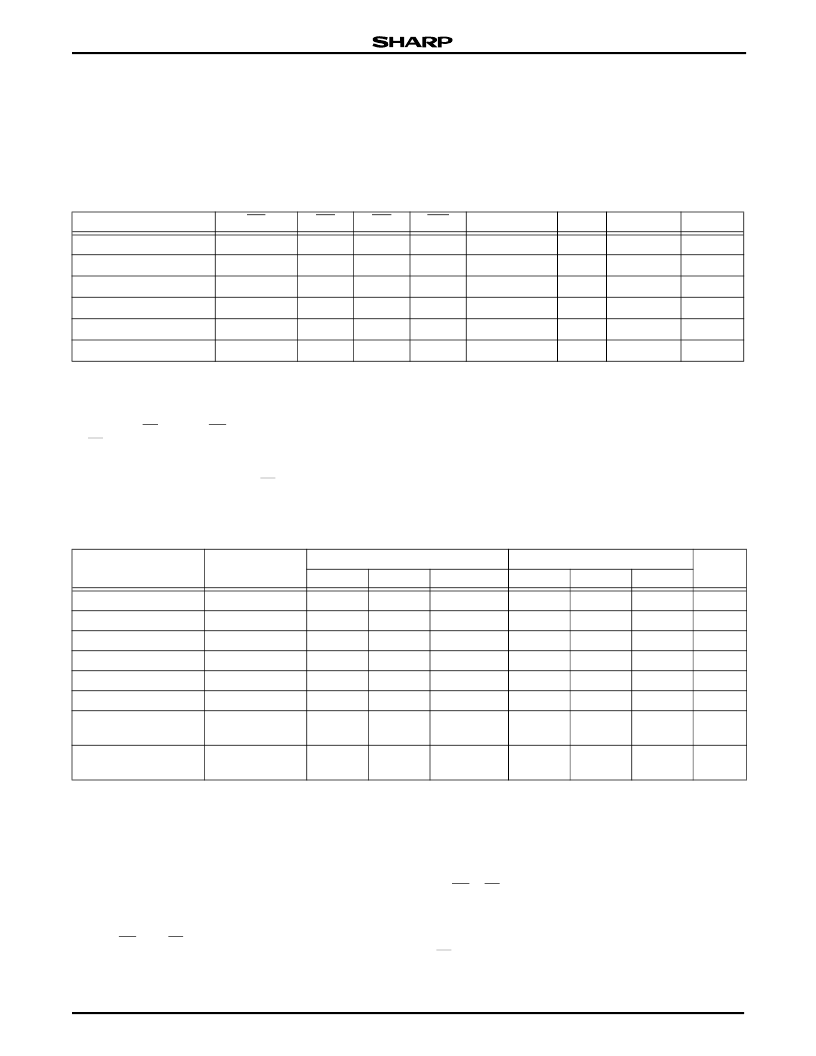
Table 5. Bus Operations
MODE
RP
CE
V
IL
V
IL
V
IH
X
V
IL
V
IL
OE
V
IL
V
IH
X
X
V
IL
V
IH
WE
V
IH
V
IH
X
X
V
IH
V
IL
ADDRESS
X
X
X
X
See Figure 3
X
V
PP
X
X
X
X
X
X
I/O
0
- I/O
15
D
OUT
HIGH Z
HIGH Z
HIGH Z
NOTES
1, 2, 3
Read
Output Disable
Standby
Deep Power-Down
Read Identifier Codes
Write
V
IH
or V
HH
V
IH
or V
HH
V
IH
or V
HH
V
IL
V
IH
or V
HH
V
IH
or V
HH
4
5
D
IN
3, 6, 7
Table 6. Command Definitions
1
COMMAND
BUS CYCLES
REQUIRED
FIRST BUS CYCLE
OPER.
2
ADDR.
3
Write
SECOND BUS CYCLE
OPER.
2
ADDR.
3
NOTES
DATA
4
FFH
DATA
4
Read Array/Reset
1
X
Read Identifier Codes
Read Status Register
Clear Status Register
Block Erase
Word Write
Block Erase and Word
Write Suspend
Block Erase and Word
Write Resume
≥
2
2
1
2
2
Write
Write
Write
Write
Write
X
X
X
BA
WA
90H
70H
50H
20H
Read
Read
IA
X
ID
5
SRD
Write
Write
BA
WA
D0H
WD
6
40H or 10H
6, 7
1
Write
X
B0H
6
1
Write
X
D0H
6
相關PDF資料 |
PDF描述 |
|---|---|
| LRS1341 | Stacked Chip 16M Flash Memory and 2M SRAM |
| LRS1805A | Stacked Chip 64M (x16) Flash Memory + 16M (x16) Smartcombo RAM |
| LRS250 | LIGHT EMITTING DIODES |
| LRS250-DO | LIGHT EMITTING DIODES |
| LRZ180-CO | Array LED 2 mm LED, Diffused |
相關代理商/技術參數(shù) |
參數(shù)描述 |
|---|---|
| LRS1341 | 制造商:SHARP 制造商全稱:Sharp Electrionic Components 功能描述:Stacked Chip 16M Flash Memory and 2M SRAM |
| LRS1342 | 制造商:Sharp Microelectronics Corporation 功能描述:COMBO 1MX16 FLASH + 128KX16 SRAM 2.7V TO 3.6V 72FBGA - Trays |
| LRS1348 | 制造商:未知廠家 制造商全稱:未知廠家 功能描述:Flash ROM |
| LRS1360 | 制造商:未知廠家 制造商全稱:未知廠家 功能描述:Flash ROM |
| LRS1360C | 制造商:未知廠家 制造商全稱:未知廠家 功能描述:MIXED MEMORY|SRAM+EEPROM|HYBRID|BGA|72PIN|PLASTIC |
發(fā)布緊急采購,3分鐘左右您將得到回復。