- 您現(xiàn)在的位置:買賣IC網(wǎng) > PDF目錄358941 > LRS1338A (Sharp Corporation) Stacked Chip 8M Flash Memory and 2M SRAM PDF資料下載
參數(shù)資料
| 型號: | LRS1338A |
| 廠商: | Sharp Corporation |
| 英文描述: | Stacked Chip 8M Flash Memory and 2M SRAM |
| 中文描述: | 堆疊芯片800萬快閃記憶體以及2M SRAM |
| 文件頁數(shù): | 10/36頁 |
| 文件大小: | 218K |
| 代理商: | LRS1338A |
第1頁第2頁第3頁第4頁第5頁第6頁第7頁第8頁第9頁當(dāng)前第10頁第11頁第12頁第13頁第14頁第15頁第16頁第17頁第18頁第19頁第20頁第21頁第22頁第23頁第24頁第25頁第26頁第27頁第28頁第29頁第30頁第31頁第32頁第33頁第34頁第35頁第36頁
LRS1338A
Stacked Chip (8M Flash & 2M SRAM)
10
Data Sheet
Bus Operation
The local CPU reads and writes flash memory in-
system. All bus cycles to or from the flash memory con-
form to standard microprocessor bus cycles.
READ
Information can be read from any block, identifier
codes or status register independent of the V
PP
volt-
age. RP can be either V
IH
or V
HH
.
The first task is to write the appropriate read mode
command (Read Array, Read Identifier Codes, or Read
Status Register) to the CUI. Upon initial device power-
up or after exit from deep power-down mode, the device
automatically resets to read array mode. Five control
pins dictate the data flow in and out of the component:
CE, OE, WE, RP and WP. CE and OE must be driven
active to obtain data at the outputs. CE is the device
selection control, and when active enables the selected
memory device. OE is the data output (I/O
0
- I/O
15
) con-
trol and when active drives the selected memory data
onto the I/O bus. WE must be at V
IH
and RP must be at
V
IH
or V
HH
. Figure 12 illustrates a read cycle.
OUTPUT DISABLE
With OE at a logic-HIGH level (V
IH
), the device out-
puts are disabled. Output pins (I/O
0
- I/O
15
) are placed
in a HIGH impedance state.
STANDBY
CE at a logic HIGH level (V
IH
) places the device in
standby mode which substantially reduces device
power consumption. I/O
0
- I/O
15
outputs are placed in
a HIGH-impedance state independent of OE. If dese-
lected during block erase or word write, the device con-
tinues functioning, and consuming active power until
the operation completes.
DEEP POWER-DOWN
RP at V
IL
initiates the deep power down mode.
In read modes, RP-LOW deselects the memory,
places output drivers in a HIGH-impedance state and
turns off all internal circuits. RP must be held LOW for
a minimum of 100 ns. Time t
PHQV
is required after
return from power-down until initial memory access
outputs are valid. After this wake-up interval, normal
operation is restored. The CUI is reset to read array
mode and status register is set to 80H.
During block erase or word write modes, RP-LOW
will abort the operation. Memory contents being altered
are no longer valid; the data may be partially erased or
written. Time t
PHWL
is required after RP goes to logic
HIGH (V
IH
) before another command can be written.
As with any automated device, it is important to
assert RP during system reset. When the system
comes out of reset, it expects to read from flash mem-
ory. Automated flash memories provide status informa-
tion when accessed during block erase or word write
modes. If a CPU reset occurs with no flash memory
reset, proper CPU initialization may not occur because
the flash memory may be providing status information
instead of array data. SHARP
’
s flash memories allow
proper CPU initialization following a system reset
through the use of RP input. In this application, RP is
controlled by the same RESET signal that resets the
system CPU.
READ IDENTIFIER CODES OPERATION
The read identifier codes operation outputs the manu-
facturer code and device codes, the system CPU can
automatically match the device with its proper algorithms.
WRITE
Writing commands to the CUI enable reading of
device data and identifier codes. They also control
inspection and clearing of the status register.
When V
CC
= V
CC1
and V
PP
= V
PPH
, the CUI addi-
tionally controls block erasure and word write. The
Block Erase command requires appropriate command
data and an address within the block to be erased. The
Word Write command requires the command and
address of the location to be written.
The CUI does not occupy an addressable memory
location. It is written when WE and CE are active. The
address and data needed to execute a command are
latched on the rising edge of WE or CE (whichever
goes HIGH first). Standard microprocessor write tim-
ings are used. Figure 13 and 14 illustrate WE and CE
controlled write operations.
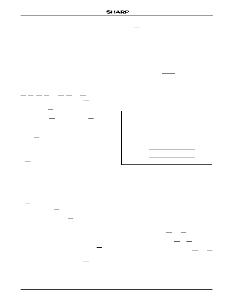
Figure 5. Device Identifier Code Memory Map
RESERVED FOR
FUTURE IMPLEMENTATION
DEVICE CODE
MANUFACTURER CODE
7FFFF
00001
00000
1338A-5
相關(guān)PDF資料 |
PDF描述 |
|---|---|
| LRS1341 | Stacked Chip 16M Flash Memory and 2M SRAM |
| LRS1805A | Stacked Chip 64M (x16) Flash Memory + 16M (x16) Smartcombo RAM |
| LRS250 | LIGHT EMITTING DIODES |
| LRS250-DO | LIGHT EMITTING DIODES |
| LRZ180-CO | Array LED 2 mm LED, Diffused |
相關(guān)代理商/技術(shù)參數(shù) |
參數(shù)描述 |
|---|---|
| LRS1341 | 制造商:SHARP 制造商全稱:Sharp Electrionic Components 功能描述:Stacked Chip 16M Flash Memory and 2M SRAM |
| LRS1342 | 制造商:Sharp Microelectronics Corporation 功能描述:COMBO 1MX16 FLASH + 128KX16 SRAM 2.7V TO 3.6V 72FBGA - Trays |
| LRS1348 | 制造商:未知廠家 制造商全稱:未知廠家 功能描述:Flash ROM |
| LRS1360 | 制造商:未知廠家 制造商全稱:未知廠家 功能描述:Flash ROM |
| LRS1360C | 制造商:未知廠家 制造商全稱:未知廠家 功能描述:MIXED MEMORY|SRAM+EEPROM|HYBRID|BGA|72PIN|PLASTIC |
發(fā)布緊急采購,3分鐘左右您將得到回復(fù)。