- 您現(xiàn)在的位置:買賣IC網(wǎng) > PDF目錄379203 > IBM038329NL6B (IBM Microeletronics) 256K x 32 Synchronous Graphics RAM(256K x 32 高性能8M位CMOS同步動(dòng)態(tài)RAM(帶內(nèi)置的圖形性能)) PDF資料下載
參數(shù)資料
| 型號(hào): | IBM038329NL6B |
| 廠商: | IBM Microeletronics |
| 英文描述: | 256K x 32 Synchronous Graphics RAM(256K x 32 高性能8M位CMOS同步動(dòng)態(tài)RAM(帶內(nèi)置的圖形性能)) |
| 中文描述: | 256K × 32同步圖形RAM(256K × 32位高性能800萬的CMOS同步動(dòng)態(tài)隨機(jī)存儲(chǔ)器(帶內(nèi)置的圖形性能)) |
| 文件頁數(shù): | 12/66頁 |
| 文件大小: | 952K |
| 代理商: | IBM038329NL6B |
第1頁第2頁第3頁第4頁第5頁第6頁第7頁第8頁第9頁第10頁第11頁當(dāng)前第12頁第13頁第14頁第15頁第16頁第17頁第18頁第19頁第20頁第21頁第22頁第23頁第24頁第25頁第26頁第27頁第28頁第29頁第30頁第31頁第32頁第33頁第34頁第35頁第36頁第37頁第38頁第39頁第40頁第41頁第42頁第43頁第44頁第45頁第46頁第47頁第48頁第49頁第50頁第51頁第52頁第53頁第54頁第55頁第56頁第57頁第58頁第59頁第60頁第61頁第62頁第63頁第64頁第65頁第66頁
IBM038329NL6B
IBM038329NP6B
256K x 32 Synchronous Graphics RAM
IBM Corporation. All rights reserved.
Use is further subject to the provisions at the end of this document.
Page 12 of 66
03K4292.E35604
Revised 3/98
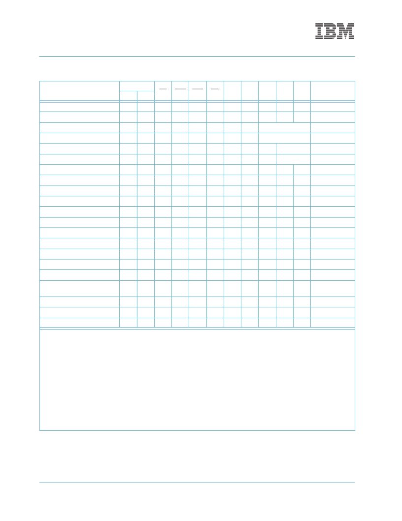
Function Truth Table
Operation
CKE
CS
RAS
CAS
WE
DSF
DQM
BA
(A
9
)
A
8
A
7
-A
0
MNE
n-1
n
Device Deselect
H
X
H
X
X
X
X
X
X
X
X
INHBT
No Operation
H
X
L
H
H
H
X
X
X
X
X
NOP
Load Mode Register
H
X
L
L
L
L
L
X
OP CODE
LMR
Load Special Mode Register
H
X
L
L
L
L
H
X
OP CODE
LSMR
Row Activate
H
X
L
L
H
H
L
X
BS
Row Addr
ACT
Row Activate w/WPB
H
X
L
L
H
H
H
X
BS
Row Addr
ACTM
Read
H
X
L
H
L
H
X
X
BS
L
Col.
RD
Read with Auto Precharge
H
X
L
H
L
H
X
X
BS
H
Col.
RDA
Write Command
H
X
L
H
L
L
L
X
BS
L
Col.
WR
Write w/ Auto Precharge
H
X
L
H
L
L
L
X
BS
H
Col.
WRA
Block Write
H
X
L
H
L
L
H
X
BS
L
Col.
BW
Block Write with Auto Precharge
H
X
L
H
L
L
H
X
BS
H
Col.
BWA
Burst Termination
H
X
L
H
H
L
X
X
X
X
X
BST
Precharge Single Bank
H
X
L
L
H
L
X
X
BS
L
X
PRE
Precharge All Banks
H
X
L
L
H
L
X
X
X
H
X
PREAL
Auto Refresh
H
H
L
L
L
H
X
X
X
X
X
REF
Self Refresh Entry
H
L
L
L
L
H
X
X
X
X
X
SREF(EN)
Self Refresh Exit
L
L
H
H
H
L
X
H
X
H
X
H
X
X
X
X
X
X
X
X
X
X
SREF(EX)
Power Down Mode (Entry)
H
L
H
X
X
X
X
X
X
X
X
PDN-(EN)
Power Down Mode (Entry)
H
L
L
H
H
H
X
X
X
X
X
PDN-(EN)
Power Down Mode (Exit)
L
H
X
X
X
X
X
X
X
X
X
PDN-(EX)
1. All inputs are latched on the rising edge of CLK.
2. LMR, LSMR, REF, and SREF commands should be issued only after both banks are deactivated (PREAL command).
3. ACT and ACTM command should be issued only after the corresponding bank has been deactivated (PRE command).
4. WR, WRA, RD, RDA should be issued after the corresponding bank has been activated (ACT command).
5. Auto Precharge command is not valid for full-page burst.
6. BW and BWA commands use Mask Register data only after ACTM command. DQM byte masking is active regardless of WPB
mask.
7. Loading Mask Register: Initiate an LSMR cycle with address pin A
5
=1 to load the Mask Register with the Mask data present on DQ
pins. Except A
5
, all other address pins must be “0” during LSMR cycle while loading the Mask Register.
8. Loading Color Register: Initiate an LSMR cycle with address pin A
6
=1 to load the Color register with the Color input data on DQ
pins. Except A
6
, all other address pins must be “0” during LSMR cycle while loading Color Register 0.
9. Any Write or Block Write cycles to the selected bank/row while active will be masked according to the contents of theMask Regis-
ter, in addition to the DQM signals and the column/byte mask information (the later for Block Writes only).
10. Block Writes are not burst oriented and always apply to the eight column locations selected by A
7
-A
3
.
相關(guān)PDF資料 |
PDF描述 |
|---|---|
| IBM038329NP6B | 256K x 32 Synchronous Graphics RAM(256K x 32 高性能8M位CMOS同步動(dòng)態(tài)RAM(帶內(nèi)置的圖形性能)) |
| IBM041812PQKB | 64K X 18 BURST SRAM(64K X 18高性能可猝發(fā)同步CMOS靜態(tài)RAM) |
| IBM041813PPLB | 64K X 18 BURST PIPELINE SRAM(1M (64K X 18)同步可猝發(fā)流水線式線式高性能靜態(tài)RAM) |
| IBM041813PQKB | 64K X 18 Burst Pipeline SRAM(1M(64K X 18)高性能同步可猝發(fā)管線式靜態(tài)RAM) |
| IBM041814PPLB | 64K X 18 BURST SRAM(1M (64K X 18)同步可猝發(fā)高性能靜態(tài)RAM) |
相關(guān)代理商/技術(shù)參數(shù) |
參數(shù)描述 |
|---|---|
| IBM038329NQ6A-7R5 | 制造商:IBM 功能描述: |
| IBM041812PQKB10 | 制造商:IBM 功能描述:* |
| IBM041812PQKB11 | 制造商:IBM 功能描述:* |
| IBM041813PQKB5 | 制造商:IBM 功能描述: |
| IBM0418A4ACLAA-4F | 制造商:IBM 功能描述: |
發(fā)布緊急采購,3分鐘左右您將得到回復(fù)。