- 您現(xiàn)在的位置:買賣IC網(wǎng) > PDF目錄1919 > ENC624J600T-I/PT (Microchip Technology)IC ETHERNET CTRLR W/SPI 64-TQFP PDF資料下載
參數(shù)資料
| 型號: | ENC624J600T-I/PT |
| 廠商: | Microchip Technology |
| 文件頁數(shù): | 57/168頁 |
| 文件大小: | 0K |
| 描述: | IC ETHERNET CTRLR W/SPI 64-TQFP |
| 視頻文件: | Fast 100 Mbps Ethernet PICtail Plus Overview |
| 標(biāo)準(zhǔn)包裝: | 1,200 |
| 控制器類型: | 以太網(wǎng)控制器(IEEE 802.3) |
| 接口: | SPI |
| 電源電壓: | 3 V ~ 3.6 V |
| 電流 - 電源: | 96mA |
| 工作溫度: | -40°C ~ 85°C |
| 安裝類型: | 表面貼裝 |
| 封裝/外殼: | 64-TQFP |
| 供應(yīng)商設(shè)備封裝: | 64-TQFP(10x10) |
| 包裝: | 帶卷 (TR) |
| 配用: | AC164132-ND - BOARD DAUGHTER PICTAIL ETHERNET |
第1頁第2頁第3頁第4頁第5頁第6頁第7頁第8頁第9頁第10頁第11頁第12頁第13頁第14頁第15頁第16頁第17頁第18頁第19頁第20頁第21頁第22頁第23頁第24頁第25頁第26頁第27頁第28頁第29頁第30頁第31頁第32頁第33頁第34頁第35頁第36頁第37頁第38頁第39頁第40頁第41頁第42頁第43頁第44頁第45頁第46頁第47頁第48頁第49頁第50頁第51頁第52頁第53頁第54頁第55頁第56頁當(dāng)前第57頁第58頁第59頁第60頁第61頁第62頁第63頁第64頁第65頁第66頁第67頁第68頁第69頁第70頁第71頁第72頁第73頁第74頁第75頁第76頁第77頁第78頁第79頁第80頁第81頁第82頁第83頁第84頁第85頁第86頁第87頁第88頁第89頁第90頁第91頁第92頁第93頁第94頁第95頁第96頁第97頁第98頁第99頁第100頁第101頁第102頁第103頁第104頁第105頁第106頁第107頁第108頁第109頁第110頁第111頁第112頁第113頁第114頁第115頁第116頁第117頁第118頁第119頁第120頁第121頁第122頁第123頁第124頁第125頁第126頁第127頁第128頁第129頁第130頁第131頁第132頁第133頁第134頁第135頁第136頁第137頁第138頁第139頁第140頁第141頁第142頁第143頁第144頁第145頁第146頁第147頁第148頁第149頁第150頁第151頁第152頁第153頁第154頁第155頁第156頁第157頁第158頁第159頁第160頁第161頁第162頁第163頁第164頁第165頁第166頁第167頁第168頁
2007 Microchip Technology Inc.
DS21993C-page 13
PIC16CR7X
2.0
MEMORY ORGANIZATION
There are two memory blocks in each of these PIC
MCUs. The Program Memory and Data Memory have
separate buses so that concurrent access can occur
and is detailed in this section. The Program Memory
can be read internally by user code (see Section 3.0
Additional information on device memory may be found
in the “PIC Mid-Range MCU Family Reference
Manual” (DS33023).
2.1
Program Memory Organization
The PIC16CR7X devices have a 13-bit program
counter capable of addressing an 8K word x 14-bit pro-
gram memory space. The PIC16CR77/76 devices
have 8K words of ROM program memory and the
PIC16CR73/74 devices have 4K words. The program
memory maps for PIC16CR7X devices are shown in
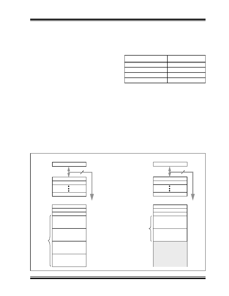
Figure 2-1. Accessing a location above the physically
implemented address will cause a wraparound.
The Reset vector is at 0000h and the interrupt vector is
at 0004h.
2.2
Data Memory Organization
The Data Memory is partitioned into multiple banks,
which contain the General Purpose Registers (GPR)
and the Special Function Registers (SFR). Bits RP1
(STATUS<6>) and RP0 (STATUS<5>) are the bank
select bits:
Each bank extends up to 7Fh (128 bytes). The lower
locations of each bank are reserved for the Special
Function Registers. Above the Special Function Regis-
ters are General Purpose Registers, implemented as
static RAM. All implemented banks contain Special
Function Registers. Some frequently used Special
Function Registers from one bank may be mirrored in
another bank for code reduction and quicker access.
2.2.1
GENERAL PURPOSE REGISTER
FILE
The register file (shown in Figure 2-2 and Figure 2-3)
can be accessed either directly, or indirectly, through
the File Select Register (FSR).
FIGURE 2-1:
PROGRAM MEMORY MAPS AND STACKS FOR PIC16CR7X DEVICES
RP1:RP0
Bank
00
0
01
1
10
2
11
3
PC<12:0>
13
0000h
0004h
0005h
Stack Level 1
Stack Level 8
Reset Vector
Interrupt Vector
On-Chip
CALL, RETURN
RETFIE, RETLW
1FFFh
Stack Level 2
Program
Memory
Page 0
Page 1
07FFh
0800h
0FFFh
1000h
17FFh
1800h
Reset Vector
Interrupt Vector
Page 0
Page 1
Page 2
Page 3
0000h
0004h
0005h
1FFFh
07FFh
0800h
0FFFh
1000h
PC<12:0>
13
Stack Level 1
Stack Level 8
CALL, RETURN
RETFIE, RETLW
Stack Level 2
Unimplemented
Read as ‘0’
On-Chip
Program
Memory
PIC16CR76/77
PIC16CR73/74
相關(guān)PDF資料 |
PDF描述 |
|---|---|
| EP1AGX90EF1152I6 | IC ARRIA GX FPGA 90K 1152FBGA |
| EP1C3T144A8N | IC CYCLONE FPGA 2910 LE 144-TQFP |
| EP1K100FC484-1N | IC ACEX 1K FPGA 100K 484-FBGA |
| EP1S80F1020C5N | IC STRATIX FPGA 80K LE 1020-FBGA |
| EP1SGX40GF1020I6 | IC STRATIX GX FPGA 40K 1020-FBGA |
相關(guān)代理商/技術(shù)參數(shù) |
參數(shù)描述 |
|---|---|
| ENC680D05B | 制造商:未知廠家 制造商全稱:未知廠家 功能描述: |
| ENC680D-05B | 制造商:未知廠家 制造商全稱:未知廠家 功能描述:STD MOV |
| ENC680D07B | 制造商:未知廠家 制造商全稱:未知廠家 功能描述: |
| ENC680D-07B | 制造商:未知廠家 制造商全稱:未知廠家 功能描述:STD MOV |
| ENC680D10B | 制造商:未知廠家 制造商全稱:未知廠家 功能描述: |
發(fā)布緊急采購,3分鐘左右您將得到回復(fù)。