- 您現(xiàn)在的位置:買賣IC網(wǎng) > PDF目錄1919 > ENC624J600T-I/PT (Microchip Technology)IC ETHERNET CTRLR W/SPI 64-TQFP PDF資料下載
參數(shù)資料
| 型號: | ENC624J600T-I/PT |
| 廠商: | Microchip Technology |
| 文件頁數(shù): | 30/168頁 |
| 文件大小: | 0K |
| 描述: | IC ETHERNET CTRLR W/SPI 64-TQFP |
| 視頻文件: | Fast 100 Mbps Ethernet PICtail Plus Overview |
| 標準包裝: | 1,200 |
| 控制器類型: | 以太網(wǎng)控制器(IEEE 802.3) |
| 接口: | SPI |
| 電源電壓: | 3 V ~ 3.6 V |
| 電流 - 電源: | 96mA |
| 工作溫度: | -40°C ~ 85°C |
| 安裝類型: | 表面貼裝 |
| 封裝/外殼: | 64-TQFP |
| 供應商設備封裝: | 64-TQFP(10x10) |
| 包裝: | 帶卷 (TR) |
| 配用: | AC164132-ND - BOARD DAUGHTER PICTAIL ETHERNET |
第1頁第2頁第3頁第4頁第5頁第6頁第7頁第8頁第9頁第10頁第11頁第12頁第13頁第14頁第15頁第16頁第17頁第18頁第19頁第20頁第21頁第22頁第23頁第24頁第25頁第26頁第27頁第28頁第29頁當前第30頁第31頁第32頁第33頁第34頁第35頁第36頁第37頁第38頁第39頁第40頁第41頁第42頁第43頁第44頁第45頁第46頁第47頁第48頁第49頁第50頁第51頁第52頁第53頁第54頁第55頁第56頁第57頁第58頁第59頁第60頁第61頁第62頁第63頁第64頁第65頁第66頁第67頁第68頁第69頁第70頁第71頁第72頁第73頁第74頁第75頁第76頁第77頁第78頁第79頁第80頁第81頁第82頁第83頁第84頁第85頁第86頁第87頁第88頁第89頁第90頁第91頁第92頁第93頁第94頁第95頁第96頁第97頁第98頁第99頁第100頁第101頁第102頁第103頁第104頁第105頁第106頁第107頁第108頁第109頁第110頁第111頁第112頁第113頁第114頁第115頁第116頁第117頁第118頁第119頁第120頁第121頁第122頁第123頁第124頁第125頁第126頁第127頁第128頁第129頁第130頁第131頁第132頁第133頁第134頁第135頁第136頁第137頁第138頁第139頁第140頁第141頁第142頁第143頁第144頁第145頁第146頁第147頁第148頁第149頁第150頁第151頁第152頁第153頁第154頁第155頁第156頁第157頁第158頁第159頁第160頁第161頁第162頁第163頁第164頁第165頁第166頁第167頁第168頁
2007 Microchip Technology Inc.
DS39599G-page 123
PIC18F2220/2320/4220/4320
12.2
Timer1 Oscillator
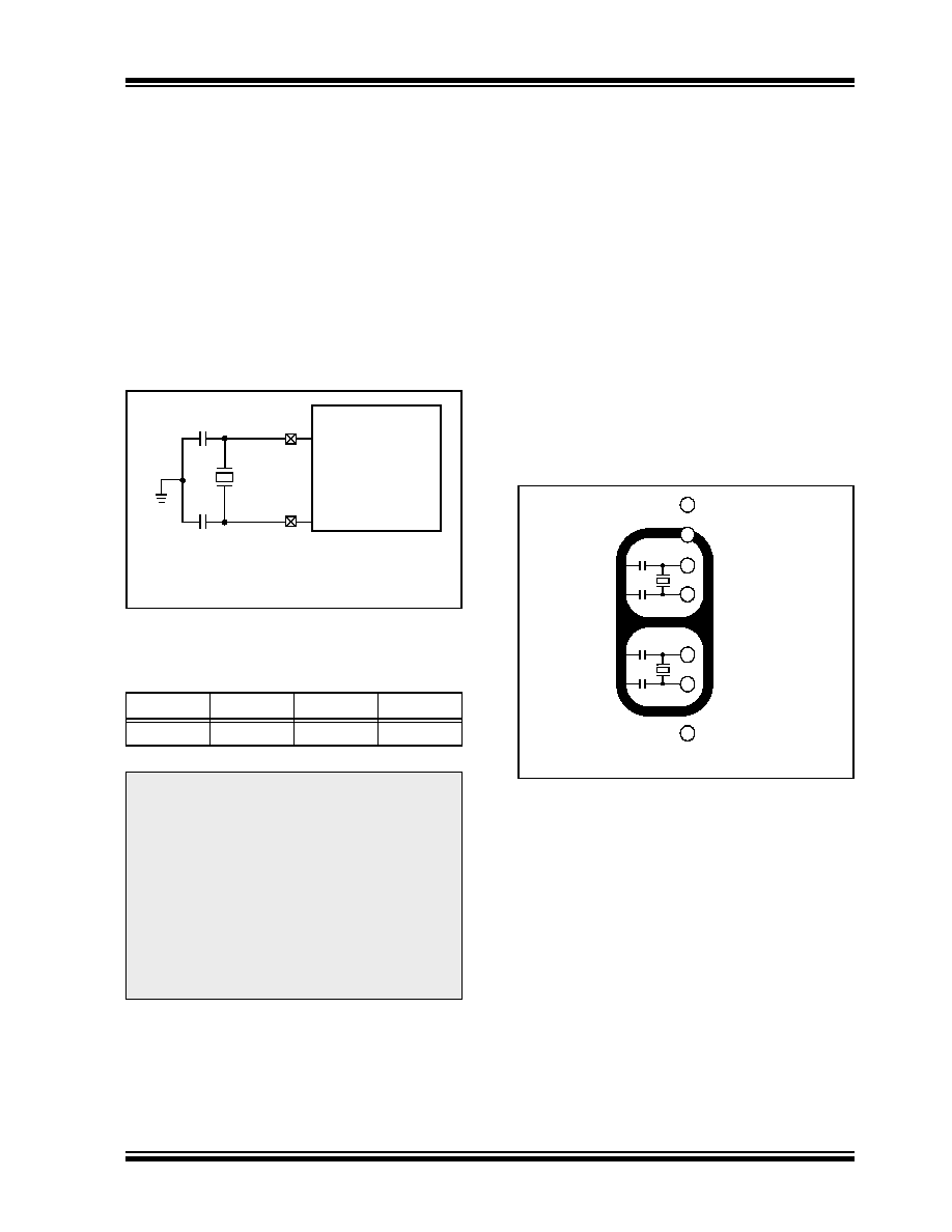
A crystal oscillator circuit is built-in between pins,
T1OSI (input) and T1OSO (amplifier output). It is
enabled by setting control bit, T1OSCEN (T1CON<3>).
The oscillator is a low-power oscillator rated for 32 kHz
crystals. It will continue to run during all power-
managed modes. The circuit for a typical LP oscillator
is shown in Figure 12-3. Table 12-1 shows the
capacitor selection for the Timer1 oscillator.
The user must provide a software time delay to ensure
proper start-up of the Timer1 oscillator.
FIGURE 12-3:
EXTERNAL COMPONENTS
FOR THE TIMER1 LP
OSCILLATOR
TABLE 12-1:
CAPACITOR SELECTION FOR
THETIMEROSCILLATOR(2,3,4)
12.3
Timer1 Oscillator Layout
Considerations
The Timer1 oscillator circuit draws very little power
during operation. Due to the low-power nature of the
oscillator, it may also be sensitive to rapidly changing
signals in close proximity.
The oscillator circuit, shown in Figure 12-3, should be
located as close as possible to the microcontroller.
There should be no circuits passing within the oscillator
circuit boundaries other than VSS or VDD.
If a high-speed circuit must be located near the oscilla-
tor (such as the CCP1 pin in output compare or PWM
mode, or the primary oscillator using the OSC2 pin), a
grounded guard ring around the oscillator circuit, as
shown in Figure 12-4, may be helpful when used on a
single-sided PCB or in addition to a ground plane.
FIGURE 12-4:
OSCILLATOR CIRCUIT
WITH GROUNDED GUARD
RING
Osc Type
Freq
C1
C2
LP
32 kHz
22 pF(1)
Note 1: Microchip suggests this value as a starting
point in validating the oscillator circuit.
2: Higher capacitance increases the stability
of the oscillator but also increases the
start-up time.
3: Since each resonator/crystal has its own
characteristics, the user should consult
the resonator/crystal manufacturer for
appropriate
values
of
external
components.
4: Capacitor values are for design guidance
only.
Note:
See the Notes with Table 12-1 for additional
information about capacitor selection.
C1
C2
XTAL
PIC18FXXXX
T1OSI
T1OSO
32.768 kHz
22 pF
VDD
OSC1
VSS
OSC2
RC0
RC1
RC2
Note: Not drawn to scale.
相關PDF資料 |
PDF描述 |
|---|---|
| EP1AGX90EF1152I6 | IC ARRIA GX FPGA 90K 1152FBGA |
| EP1C3T144A8N | IC CYCLONE FPGA 2910 LE 144-TQFP |
| EP1K100FC484-1N | IC ACEX 1K FPGA 100K 484-FBGA |
| EP1S80F1020C5N | IC STRATIX FPGA 80K LE 1020-FBGA |
| EP1SGX40GF1020I6 | IC STRATIX GX FPGA 40K 1020-FBGA |
相關代理商/技術參數(shù) |
參數(shù)描述 |
|---|---|
| ENC680D05B | 制造商:未知廠家 制造商全稱:未知廠家 功能描述: |
| ENC680D-05B | 制造商:未知廠家 制造商全稱:未知廠家 功能描述:STD MOV |
| ENC680D07B | 制造商:未知廠家 制造商全稱:未知廠家 功能描述: |
| ENC680D-07B | 制造商:未知廠家 制造商全稱:未知廠家 功能描述:STD MOV |
| ENC680D10B | 制造商:未知廠家 制造商全稱:未知廠家 功能描述: |
發(fā)布緊急采購,3分鐘左右您將得到回復。