- 您現(xiàn)在的位置:買賣IC網(wǎng) > PDF目錄1919 > ENC624J600T-I/PT (Microchip Technology)IC ETHERNET CTRLR W/SPI 64-TQFP PDF資料下載
參數(shù)資料
| 型號(hào): | ENC624J600T-I/PT |
| 廠商: | Microchip Technology |
| 文件頁數(shù): | 13/168頁 |
| 文件大?。?/td> | 0K |
| 描述: | IC ETHERNET CTRLR W/SPI 64-TQFP |
| 視頻文件: | Fast 100 Mbps Ethernet PICtail Plus Overview |
| 標(biāo)準(zhǔn)包裝: | 1,200 |
| 控制器類型: | 以太網(wǎng)控制器(IEEE 802.3) |
| 接口: | SPI |
| 電源電壓: | 3 V ~ 3.6 V |
| 電流 - 電源: | 96mA |
| 工作溫度: | -40°C ~ 85°C |
| 安裝類型: | 表面貼裝 |
| 封裝/外殼: | 64-TQFP |
| 供應(yīng)商設(shè)備封裝: | 64-TQFP(10x10) |
| 包裝: | 帶卷 (TR) |
| 配用: | AC164132-ND - BOARD DAUGHTER PICTAIL ETHERNET |
第1頁第2頁第3頁第4頁第5頁第6頁第7頁第8頁第9頁第10頁第11頁第12頁當(dāng)前第13頁第14頁第15頁第16頁第17頁第18頁第19頁第20頁第21頁第22頁第23頁第24頁第25頁第26頁第27頁第28頁第29頁第30頁第31頁第32頁第33頁第34頁第35頁第36頁第37頁第38頁第39頁第40頁第41頁第42頁第43頁第44頁第45頁第46頁第47頁第48頁第49頁第50頁第51頁第52頁第53頁第54頁第55頁第56頁第57頁第58頁第59頁第60頁第61頁第62頁第63頁第64頁第65頁第66頁第67頁第68頁第69頁第70頁第71頁第72頁第73頁第74頁第75頁第76頁第77頁第78頁第79頁第80頁第81頁第82頁第83頁第84頁第85頁第86頁第87頁第88頁第89頁第90頁第91頁第92頁第93頁第94頁第95頁第96頁第97頁第98頁第99頁第100頁第101頁第102頁第103頁第104頁第105頁第106頁第107頁第108頁第109頁第110頁第111頁第112頁第113頁第114頁第115頁第116頁第117頁第118頁第119頁第120頁第121頁第122頁第123頁第124頁第125頁第126頁第127頁第128頁第129頁第130頁第131頁第132頁第133頁第134頁第135頁第136頁第137頁第138頁第139頁第140頁第141頁第142頁第143頁第144頁第145頁第146頁第147頁第148頁第149頁第150頁第151頁第152頁第153頁第154頁第155頁第156頁第157頁第158頁第159頁第160頁第161頁第162頁第163頁第164頁第165頁第166頁第167頁第168頁
2010 Microchip Technology Inc.
DS39935C-page 9
ENC424J600/624J600
2.0
EXTERNAL CONNECTIONS
2.1
Oscillator
ENC424J600/624J600 devices are designed to
operate from a fixed 25 MHz clock input. This clock can
be generated by an external CMOS clock oscillator or
a parallel resonant, fundamental mode 25 MHz crystal
attached to the OSC1 and OSC2 pins. Use of a crystal,
rated for series resonant operation, will oscillate at an
incorrect frequency. To comply with IEEE 802.3 Ethernet
timing requirements, the clock must have no more than
±50 ppm of total error; avoid using resonators or clock
generators that exceed this margin.
When clocking the device using a crystal, follow the
connections shown in Figure 2-1. When using a CMOS
clock oscillator or other external clock source, follow
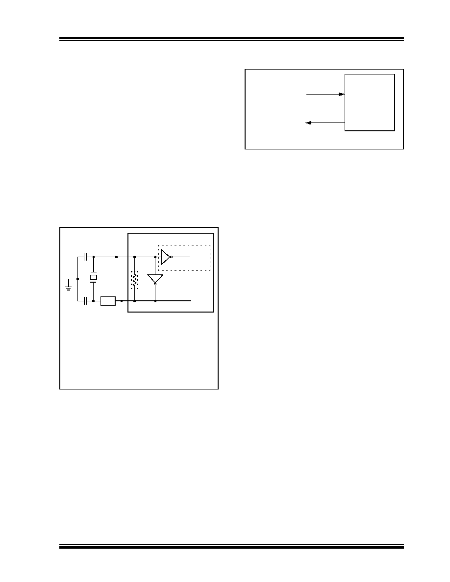
FIGURE 2-1:
CRYSTAL OSCILLATOR
OPERATION
FIGURE 2-2:
EXTERNAL CLOCK
SOURCE
2.2
CLKOUT Pin
The Clock Out pin (CLKOUT) is provided for use as the
host controller clock or as a clock source for other
devices in the system. Its use is optional.
The 25 MHz clock applied to OSC1 is multiplied by a
PLL to internally generate a 100 MHz base clock. This
100 MHz clock is driven through a configurable
postscaler to yield a wide range of different CLKOUT
frequencies. The PLL multiplication adds clock jitter,
subject to the PLL jitter specification in Section 17.0
“Electrical Characteristics”. However, the postscaler
ensures that the clock will have a nearly ideal duty
cycle.
The CLKOUT function is enabled and the postscaler is
selected via the COCON<3:0> bits (ECON2<11:8>).
To create a clean clock signal, the CLKOUT output and
COCON bits are unaffected by all resets and
power-down modes. The CLKOUT function is enabled
out of POR and defaults to producing a 4 MHz clock.
This allows the device to directly clock the host
processor.
When the COCON bits are written with a new
configuration, the CLKOUT output transitions to the
new frequency without producing any glitches. No high
or low pulses with a shorter period than the original or
new clock are generated.
C1(3)
C2(3)
XTAL
OSC2
RS(1)
OSC1
RF(2)
To Internal Logic
Note 1: A series resistor, RS, may be required for
crystals with a low drive strength specification
or when using large loading capacitors.
2: The feedback resistor, RF , is typically 1.5 M
approx.
3: The load capacitors’ value should be derived
from the capacitive loading specification
provided by the crystal manufacture.
ENCX24J600
3.3V Clock from
External System(1)
OSC1
OSC2
Open
Note 1: Duty cycle restrictions must be observed.
ENCX24J600
相關(guān)PDF資料 |
PDF描述 |
|---|---|
| EP1AGX90EF1152I6 | IC ARRIA GX FPGA 90K 1152FBGA |
| EP1C3T144A8N | IC CYCLONE FPGA 2910 LE 144-TQFP |
| EP1K100FC484-1N | IC ACEX 1K FPGA 100K 484-FBGA |
| EP1S80F1020C5N | IC STRATIX FPGA 80K LE 1020-FBGA |
| EP1SGX40GF1020I6 | IC STRATIX GX FPGA 40K 1020-FBGA |
相關(guān)代理商/技術(shù)參數(shù) |
參數(shù)描述 |
|---|---|
| ENC680D05B | 制造商:未知廠家 制造商全稱:未知廠家 功能描述: |
| ENC680D-05B | 制造商:未知廠家 制造商全稱:未知廠家 功能描述:STD MOV |
| ENC680D07B | 制造商:未知廠家 制造商全稱:未知廠家 功能描述: |
| ENC680D-07B | 制造商:未知廠家 制造商全稱:未知廠家 功能描述:STD MOV |
| ENC680D10B | 制造商:未知廠家 制造商全稱:未知廠家 功能描述: |
發(fā)布緊急采購,3分鐘左右您將得到回復(fù)。