- 您現(xiàn)在的位置:買賣IC網(wǎng) > PDF目錄385639 > MT48V2M32LFFC (Micron Technology, Inc.) 512K x 32 x 4 banks 2.5V SDRAM(2.5V,512K x 32 x 4組同步動態(tài)RAM) PDF資料下載
參數(shù)資料
| 型號: | MT48V2M32LFFC |
| 廠商: | Micron Technology, Inc. |
| 英文描述: | 512K x 32 x 4 banks 2.5V SDRAM(2.5V,512K x 32 x 4組同步動態(tài)RAM) |
| 中文描述: | 為512k × 32 × 4銀行2.5V的內(nèi)存電壓(2.5V,512K采樣× 32 × 4組同步動態(tài)RAM)的 |
| 文件頁數(shù): | 19/50頁 |
| 文件大?。?/td> | 1058K |
| 代理商: | MT48V2M32LFFC |
第1頁第2頁第3頁第4頁第5頁第6頁第7頁第8頁第9頁第10頁第11頁第12頁第13頁第14頁第15頁第16頁第17頁第18頁當(dāng)前第19頁第20頁第21頁第22頁第23頁第24頁第25頁第26頁第27頁第28頁第29頁第30頁第31頁第32頁第33頁第34頁第35頁第36頁第37頁第38頁第39頁第40頁第41頁第42頁第43頁第44頁第45頁第46頁第47頁第48頁第49頁第50頁
19
64Mb: x32 SDRAM, 2.5V
BatRam_25V.p65 – Rev. 0.7, Pub. 2/01
Micron Technology, Inc., reserves the right to change products or specifications without notice.
2001, Micron Technology, Inc.
64Mb: x32, 2.5V
SDRAM
PRELIMINARY
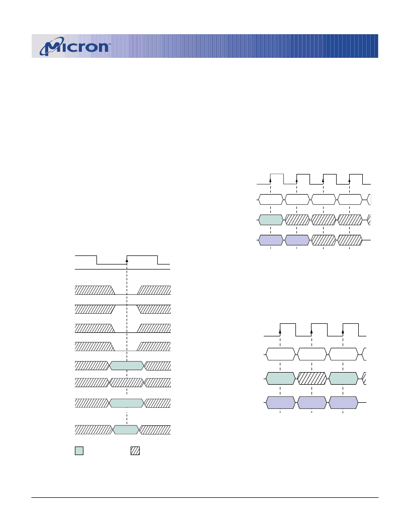
Figure 15
WRITE To WRITE
Figure 14
WRITE Burst
Figure 13
WRITE Command
CS#
WE#
CAS#
RAS#
CKE
CLK
COLUMN
DON’T CARE
HIGH
ENABLE AUTO PRECHARGE
DISABLE AUTO PRECHARGE
ABANK
A0–A7
A10
BA0, 1
A8, A9
VALID ADDRESS
CLK
DQ
D
IN
n
T2
T1
T3
T0
COMMAND
ADDRESS
NOP
NOP
WRITE
D
IN
n
+ 1
NOP
BANK,
COL
n
NOTE:
Burst length = 2. DQM is LOW.
CLK
DQ
T2
T1
T0
COMMAND
ADDRESS
NOP
WRITE
WRITE
BANK,
COL
n
BANK,
COL
b
D
IN
n
D
IN
n
+ 1
D
IN
b
NOTE:
DQM is LOW.
Each WRITE
command may be to any bank.
WRITEs
WRITE bursts are initiated with a WRITE command,
as shown in Figure 13.
The starting column and bank addresses are pro-
vided with the WRITE command, and auto precharge
is either enabled or disabled for that access. If auto
precharge is enabled, the row being accessed is
precharged at the completion of the burst. For the ge-
neric WRITE commands used in the following illustra-
tions, auto precharge is disabled.
During WRITE bursts, the first valid data-in ele-
ment will be registered coincident with the WRITE com-
mand. Subsequent data elements will be registered on
each successive positive clock edge. Upon completion
of a fixed-length burst, assuming no other commands
have been initiated, the DQs will remain High-Z and
any additional input data will be ignored (see Figure
14). A full-page burst will continue until terminated.
(At the end of the page, it will wrap to column 0 and
continue.)
Data for any WRITE burst may be truncated with a
subsequent WRITE command, and data for a fixed-
length WRITE burst may be immediately followed by
data for a WRITE command. The new WRITE command
can be issued on any clock following the previous WRITE
command, and the data provided coincident with the
new command applies to the new command. An ex-
ample is shown in Figure 15. Data
n
+ 1 is either the last
of a burst of two or the last desired of a longer burst.
This 64Mb SDRAM uses a pipelined architecture and
therefore does not require the 2
n
rule associated with a
prefetch architecture. A WRITE command can be initi-
相關(guān)PDF資料 |
PDF描述 |
|---|---|
| MT48V4M32LFFC | SYNCHRONOUS DRAM |
| MT49H16M16 | THERMISTOR PTC 100OHM 110DEG RAD |
| MT49H16M16FM | REDUCED LATENCY DRAM RLDRAM |
| MT49H8M32 | THERMISTOR PTC 100OHM 120DEG RAD |
| MT49H8M32FM | REDUCED LATENCY DRAM RLDRAM |
相關(guān)代理商/技術(shù)參數(shù) |
參數(shù)描述 |
|---|---|
| MT48V32M16S2FG-10 | 制造商:Micron Technology Inc 功能描述:32MX16 SSDRAM PLASTIC 2BOC 2.5V - Trays |
| MT48V32M16S2FG-8 ES | 制造商:Micron Technology Inc 功能描述:DRAM CHIP MOBILE SDRAM 512MBIT 2.5V 54FBGA - Bulk |
發(fā)布緊急采購,3分鐘左右您將得到回復(fù)。