- 您現(xiàn)在的位置:買(mǎi)賣(mài)IC網(wǎng) > PDF目錄298813 > AD9874ABSTZ (ANALOG DEVICES INC) SPECIALTY TELECOM CIRCUIT, PQFP48 PDF資料下載
參數(shù)資料
| 型號(hào): | AD9874ABSTZ |
| 廠商: | ANALOG DEVICES INC |
| 元件分類: | 通信及網(wǎng)絡(luò) |
| 英文描述: | SPECIALTY TELECOM CIRCUIT, PQFP48 |
| 封裝: | PLASTIC, MS-026BBC, LQFP-48 |
| 文件頁(yè)數(shù): | 7/40頁(yè) |
| 文件大?。?/td> | 1682K |
| 代理商: | AD9874ABSTZ |
第1頁(yè)第2頁(yè)第3頁(yè)第4頁(yè)第5頁(yè)第6頁(yè)當(dāng)前第7頁(yè)第8頁(yè)第9頁(yè)第10頁(yè)第11頁(yè)第12頁(yè)第13頁(yè)第14頁(yè)第15頁(yè)第16頁(yè)第17頁(yè)第18頁(yè)第19頁(yè)第20頁(yè)第21頁(yè)第22頁(yè)第23頁(yè)第24頁(yè)第25頁(yè)第26頁(yè)第27頁(yè)第28頁(yè)第29頁(yè)第30頁(yè)第31頁(yè)第32頁(yè)第33頁(yè)第34頁(yè)第35頁(yè)第36頁(yè)第37頁(yè)第38頁(yè)第39頁(yè)第40頁(yè)
REV. A
AD9874
–15–
SERIAL PORT INTERFACE (SPI)
The serial port of the AD9874 has 3-wire or 4-wire SPI capability,
allowing read/write access to all registers that configure the
device’s internal parameters. The default 3-wire serial commu-
nication port consists of a clock (PC), peripheral enable (PE), and
bidirectional data (PD) signal. The inputs to PC, PE, and PD
contain a Schmitt trigger with a nominal hysteresis of 0.4 V
centered about the digital interface supply (i.e., VDDH/2).
A 4-wire SPI interface can be enabled by setting the MSB of the
SSICRB register (Reg. 0x19, Bit 7), resulting in the output data
also appearing on the DOUTB pin. Note that since the default
power-up state sets DOUTB low, bus contention is possible for
systems sharing the SPI output line. To avoid any bus contention,
the DOUTB pin can be three-stated by setting the fourth control
bit in the three-state bit (Reg 0x3B, Bit 3). This bit can then be
toggled to gain access to the shared SPI output line.
An 8-bit instruction header must accompany each read and
write SPI operation. Only the write operation supports an auto-
increment mode, allowing the entire chip to be configured in a
single write operation. The instruction header is shown in
Table II. It includes a read/not-write indicator bit, six address
bits, and a don’t care bit. The data bits immediately follow the
instruction header for both read and write operations. Note that
the address and data are always given MSB first.
Table II. Instruction Header Information
MSB
LSB
I7
I6
I5
I4
I3
I2
I1
I0
R/W
A5
A4
A3
A2
A1
A0
X
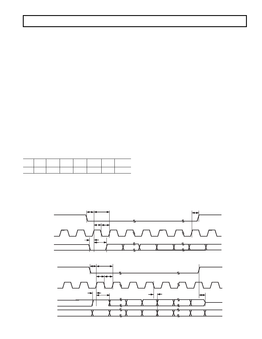
Figure 1a illustrates the timing requirements for a write opera-
tion to the SPI port. After the peripheral enable (PE) signal goes
low, data (PD) pertaining to the instruction header is read on
the rising edges of the clock (PC). To initiate a write operation,
the read/not-write bit is set low. After the instruction header is
read, the eight data bits pertaining to the specified register are
shifted into the data pin (PD) on the rising edge of the next
eight clock cycles. PE stays low during the operation and goes
high at the end of the transfer. If PE rises before the eight clock
cycles have passed, the operation is aborted.
If PE stays low for an additional eight clock cycles, the destina-
tion address is incremented and another eight bits of data are
shifted in. Again, should PE rise early, the current byte is
ignored. By using this implicit addressing mode, the entire
chip can be configured with a single write operation. Regis-
ters identified as being subject to frequent updates, namely
those associated with power control and AGC operation, have
been assigned adjacent addresses to minimize the time required
to update them. Note that multibyte registers are big-endian
(the most significant byte has the lower address) and are updated
when a write to the least significant byte occurs.
Figure 1b illustrates the timing for a read operation to the SPI
port. Although the AD9874 does not require read access for
proper operation, it is often useful in the product development
phase or for system authentication. Note that the readback
enable bit (Register 0x3A, Bit 3) must be set for a read opera-
tion with a 3-wire SPI interface. After the peripheral enable
(PE) signal goes low, data (PD) pertaining to the instruction
header is read on the rising edges of the clock (PC). A read
operation occurs if the read/not-write indicator is set high. After
the address bits of the instruction header are read, the eight data
bits pertaining to the specified register are shifted out of the
data pin (PD) on the falling edges of the next eight clock cycles.
If the 4-wire SPI interface is enabled, the eight data bits will
also appear on the DOUTB pin with the same timing relation-
ship as those appearing at PD. After the last data bit is shifted
out, the user should return PE high, causing PD to become
three-stated and return to its normal status as an input pin.
Since the auto increment mode is not supported for read opera-
tions, an instruction header is required for each register read
operation and PE must return high before initiating the next
read operation.
PC
PE
PD
A5
D7
D6
D0
A0
DON’T
CARE
D1
R/W
A1
tCLK
tHI
tLOW
tS
tEZ
tDS
tDH
tDV
DOUTB
D7
D6
D0
DON’T
CARE
D1
DON’T
CARE
DON’T
CARE
DON’T
CARE
DON’T
CARE
DON’T
CARE
Figure 1b. SPI Read Operation Timing
PC
PE
PD
A5
A4
D7
D6
D0
A0
DON’T
CARE
D1
R/W
tDS
tDH
tCLK
tHI
tLOW
tS
tH
Figure 1a. SPI Write Operation Timing
相關(guān)PDF資料 |
PDF描述 |
|---|---|
| AD9874ABSTZRL | SPECIALTY TELECOM CIRCUIT, PQFP48 |
| ADC0831CIWM | 1-CH 8-BIT SUCCESSIVE APPROXIMATION ADC, SERIAL ACCESS, PDSO14 |
| ADE7116ASTZF8-RL | SPECIALTY ANALOG CIRCUIT, PQFP64 |
| ADE7753ARSZRL | SPECIALTY ANALOG CIRCUIT, PDSO20 |
| ADEX-R10+ | 10 MHz - 1000 MHz RF/MICROWAVE DOUBLE BALANCED MIXER, 8.3 dB CONVERSION LOSS-MAX |
相關(guān)代理商/技術(shù)參數(shù) |
參數(shù)描述 |
|---|---|
| AD9874BST | 制造商:Rochester Electronics LLC 功能描述:- Tape and Reel |
| AD9874EB | 制造商:AD 制造商全稱:Analog Devices 功能描述:IF Digitizing Subsystem |
| AD9874-EB | 制造商:Analog Devices 功能描述: |
| AD9874-EBZ | 功能描述:BOARD EVAL FOR AD9874 制造商:analog devices inc. 系列:- 零件狀態(tài):有效 類型:數(shù)字轉(zhuǎn)換器 頻率:10MHz ~ 300MHz 配套使用產(chǎn)品/相關(guān)產(chǎn)品:AD9874 所含物品:板 標(biāo)準(zhǔn)包裝:1 |
| AD9875 | 制造商:AD 制造商全稱:Analog Devices 功能描述:Broadband Modem Mixed-Signal Front End |
發(fā)布緊急采購(gòu),3分鐘左右您將得到回復(fù)。