- 您現(xiàn)在的位置:買賣IC網(wǎng) > PDF目錄385949 > TSB42AA4PDT (Texas Instruments, Inc.) IEEE 1394 A CONSUMER ELECTRONICS LINK LAYER CONTROLLER PDF資料下載
參數(shù)資料
| 型號: | TSB42AA4PDT |
| 廠商: | Texas Instruments, Inc. |
| 英文描述: | IEEE 1394 A CONSUMER ELECTRONICS LINK LAYER CONTROLLER |
| 中文描述: | 1394消費(fèi)電子產(chǎn)品鏈路層控制器 |
| 文件頁數(shù): | 57/183頁 |
| 文件大小: | 798K |
| 代理商: | TSB42AA4PDT |
第1頁第2頁第3頁第4頁第5頁第6頁第7頁第8頁第9頁第10頁第11頁第12頁第13頁第14頁第15頁第16頁第17頁第18頁第19頁第20頁第21頁第22頁第23頁第24頁第25頁第26頁第27頁第28頁第29頁第30頁第31頁第32頁第33頁第34頁第35頁第36頁第37頁第38頁第39頁第40頁第41頁第42頁第43頁第44頁第45頁第46頁第47頁第48頁第49頁第50頁第51頁第52頁第53頁第54頁第55頁第56頁當(dāng)前第57頁第58頁第59頁第60頁第61頁第62頁第63頁第64頁第65頁第66頁第67頁第68頁第69頁第70頁第71頁第72頁第73頁第74頁第75頁第76頁第77頁第78頁第79頁第80頁第81頁第82頁第83頁第84頁第85頁第86頁第87頁第88頁第89頁第90頁第91頁第92頁第93頁第94頁第95頁第96頁第97頁第98頁第99頁第100頁第101頁第102頁第103頁第104頁第105頁第106頁第107頁第108頁第109頁第110頁第111頁第112頁第113頁第114頁第115頁第116頁第117頁第118頁第119頁第120頁第121頁第122頁第123頁第124頁第125頁第126頁第127頁第128頁第129頁第130頁第131頁第132頁第133頁第134頁第135頁第136頁第137頁第138頁第139頁第140頁第141頁第142頁第143頁第144頁第145頁第146頁第147頁第148頁第149頁第150頁第151頁第152頁第153頁第154頁第155頁第156頁第157頁第158頁第159頁第160頁第161頁第162頁第163頁第164頁第165頁第166頁第167頁第168頁第169頁第170頁第171頁第172頁第173頁第174頁第175頁第176頁第177頁第178頁第179頁第180頁第181頁第182頁第183頁
45
4.2.1.2
MPEG2 Time Stamp Calculation on Receive
Receiving packets with time stamps works similarly to the transmit process. When a packet with a time
stamp is received, the time stamp is captured and compared to the current cycle timer value. The time stamp
determines when ceLynx releases the packet data to the application.
If receive aging is enabled, the received packet is flushed from the FIFO if its time stamp value has expired.
The time stamp used for aging, is the received time stamp plus a time stamp offset.
4.2.2
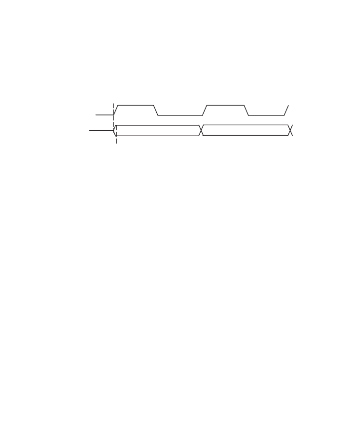
Time Stamp on Transmit to 1394 DV Data
DV_Frame_In
DV Frame 1
DV Frame 2
Time Stamp Value Is Calculated
Time Stamp Is Placed
At Next Start Of Frame
Figure 45. DV Transmit Timing
In Figure 45 the DV_Frame_In (programmable at GPIO) is used to create the time stamp for a DV packet.
The signal should be 29.97 Hz for NTSC and 25 Hz for PAL, 50% duty cycle. The cycle timer is recorded
at the time the DV_frame_In signal goes active. The value of the time stamp defined in IEC61883-2 is
determined from the recorded value of the cycle timer register and transmit offset. The time stamp is then
added to the next start of frame packet transmitted.
The DV_frame_In signal should be close to the start of a new frame or the transmit offset must be large
enough to compensate for the delay.
The time stamp is calculated by adding an offset to the value of the cycle timer register. This offset is
programmed in DB(N) CFG2 register. The 16 bit time stamp value is placed in the SYT field of the CIP
header. The least significant 12 bits after the addition of cycle timer register and DB(N) CFG register is
lowadd
. The four most significant bits after the addition is
highadd
.
The time stamp can be placed in the first data packet of the frame (empty or full) or in the first full data packet
of the frame. This is controlled by the TXDP(N) CFG register.
The cycle timer register is made up of the cycle count (4 most significant bits) and the cycle offset (12 least
significant bits). The cycle-offset portion of the cycle timer register is modulo 3072. Each time this counter
wraps around it signals the beginning of a new isochronous cycle. For a cycle master device, a cycle start
packet is transmitted at the beginning of each new isochronous cycle. For a non-cycle master device a cycle
start is decoded from a received cycle start packet.
Highadd specifies the offset in number of isochronous cycles, and lowadd specifies an offset into an
isochronous cycle. If the computation results in a lowadd which is less than 3072 (125
μ
s) then the resultant
time stamp is simply highadd and lowadd. If the computation results in a lowadd which is equal to or greater
than 3072 then the resultant time stamp is highadd + 1 and the difference between the computed lowadd
and 3072.
相關(guān)PDF資料 |
PDF描述 |
|---|---|
| TSB42AA4PGE | IEEE 1394 A CONSUMER ELECTRONICS LINK LAYER CONTROLLER |
| TSB42AA9I | STORAGELYNX 1394 LINK-LAYER CONTROLLER FOR ATA/ATAPI STORAGE PRODUCTS |
| TSB42AA9IPZT | STORAGELYNX 1394 LINK-LAYER CONTROLLER FOR ATA/ATAPI STORAGE PRODUCTS |
| TSB42AB4I | IEEE 1394 A CONSUMER ELECTRONICS LINK LAYER CONTROLLER |
| TSB42AB4PGE | IEEE 1394 A CONSUMER ELECTRONICS LINK LAYER CONTROLLER |
相關(guān)代理商/技術(shù)參數(shù) |
參數(shù)描述 |
|---|---|
| TSB42AA4PDTG4 | 功能描述:1394 接口集成電路 Link Layer Cntrlr RoHS:否 制造商:Texas Instruments 類型:Link Layer Controller 工作電源電壓: 封裝 / 箱體:LQFP 封裝:Tray |
| TSB42AA4PDTR | 制造商:Texas Instruments 功能描述: |
| TSB42AA4PGE | 制造商:TI 制造商全稱:Texas Instruments 功能描述:IEEE 1394 A CONSUMER ELECTRONICS LINK LAYER CONTROLLER |
| TSB42AA4PGER | 制造商:Rochester Electronics LLC 功能描述:- Bulk |
| TSB42AA9 | 制造商:TI 制造商全稱:Texas Instruments 功能描述:STORAGELYNX 1394 LINK-LAYER CONTROLLER FOR ATA/ATAPI STORAGE PRODUCTS |
發(fā)布緊急采購,3分鐘左右您將得到回復(fù)。