- 您現(xiàn)在的位置:買賣IC網(wǎng) > PDF目錄385949 > TSB42AA4PDT (Texas Instruments, Inc.) IEEE 1394 A CONSUMER ELECTRONICS LINK LAYER CONTROLLER PDF資料下載
參數(shù)資料
| 型號: | TSB42AA4PDT |
| 廠商: | Texas Instruments, Inc. |
| 英文描述: | IEEE 1394 A CONSUMER ELECTRONICS LINK LAYER CONTROLLER |
| 中文描述: | 1394消費電子產(chǎn)品鏈路層控制器 |
| 文件頁數(shù): | 101/183頁 |
| 文件大小: | 798K |
| 代理商: | TSB42AA4PDT |
第1頁第2頁第3頁第4頁第5頁第6頁第7頁第8頁第9頁第10頁第11頁第12頁第13頁第14頁第15頁第16頁第17頁第18頁第19頁第20頁第21頁第22頁第23頁第24頁第25頁第26頁第27頁第28頁第29頁第30頁第31頁第32頁第33頁第34頁第35頁第36頁第37頁第38頁第39頁第40頁第41頁第42頁第43頁第44頁第45頁第46頁第47頁第48頁第49頁第50頁第51頁第52頁第53頁第54頁第55頁第56頁第57頁第58頁第59頁第60頁第61頁第62頁第63頁第64頁第65頁第66頁第67頁第68頁第69頁第70頁第71頁第72頁第73頁第74頁第75頁第76頁第77頁第78頁第79頁第80頁第81頁第82頁第83頁第84頁第85頁第86頁第87頁第88頁第89頁第90頁第91頁第92頁第93頁第94頁第95頁第96頁第97頁第98頁第99頁第100頁當前第101頁第102頁第103頁第104頁第105頁第106頁第107頁第108頁第109頁第110頁第111頁第112頁第113頁第114頁第115頁第116頁第117頁第118頁第119頁第120頁第121頁第122頁第123頁第124頁第125頁第126頁第127頁第128頁第129頁第130頁第131頁第132頁第133頁第134頁第135頁第136頁第137頁第138頁第139頁第140頁第141頁第142頁第143頁第144頁第145頁第146頁第147頁第148頁第149頁第150頁第151頁第152頁第153頁第154頁第155頁第156頁第157頁第158頁第159頁第160頁第161頁第162頁第163頁第164頁第165頁第166頁第167頁第168頁第169頁第170頁第171頁第172頁第173頁第174頁第175頁第176頁第177頁第178頁第179頁第180頁第181頁第182頁第183頁
64
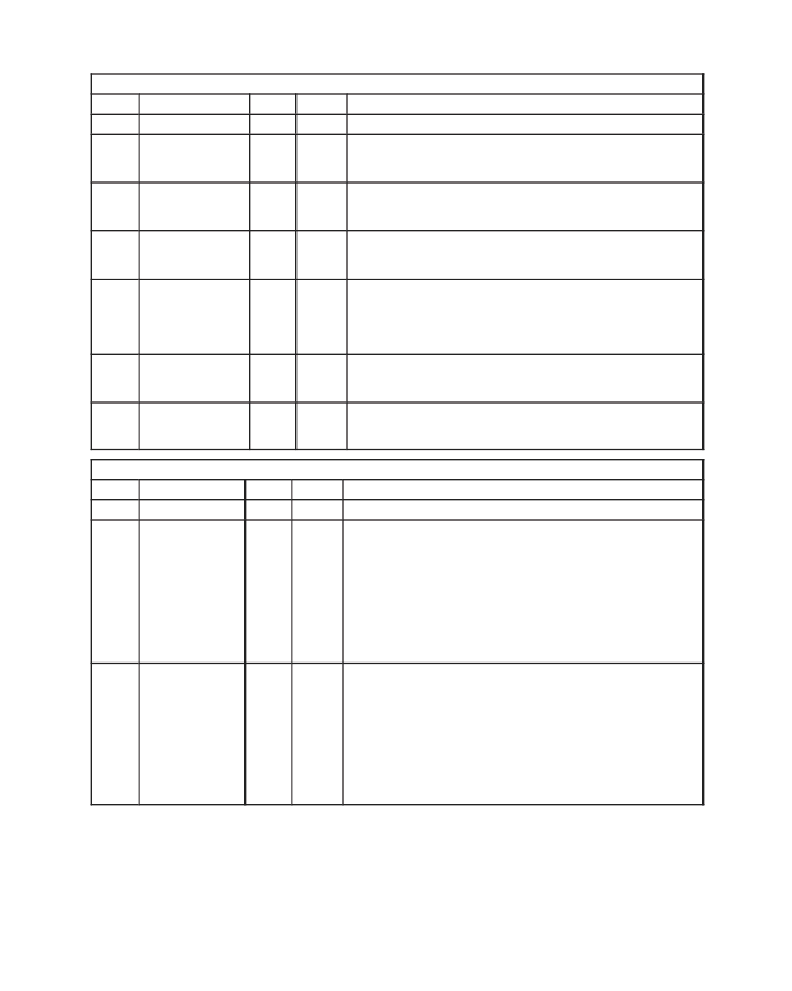
0x004 PINCFG – Pin Configuration (Continued)
BIT
NAME
TYPE
RESET
FUNCTION
7:6
RSVD
R0
0
Reserved – A write to this location has no effect. A read returns 0s.
5
MCACKZPOL
W
0
Programmable microcontroller acknowledge polarity The value
written to this location indicates the active level of the MCIF_ACKZ
pin. 1active high, 0active low
4
MCACKZPOL
R
0
Programmable microcontroller acknowledge polarity The value
contained in this location indicates the active level of the
MCIF_ACKZ pin. 1active high, 0active low
3
MCSTRBZPOL
RW
0
Programmable microcontroller data strobe polarity The value
written to this location indicates the active level of the MCIF_STRBZ
pin. 1active high, 0active low
2
MCRWPOL
RW
1
Programmable microcontroller read/write polarity The value
written to this location indicates the active level of the MCIF_RWZ
pin.
When this bit is set to 1: Read 1 Write 0
When this bit is set to 0: Read 0 Write 1
1
MCCSZPOL
RW
0
Programmable microcontroller chip select polarity The value
written to this location indicates the active level of the MCIF_CSZ
pin. 1active high, 0active low
0
MCS32ZPOL
RW
0
Programmable microcontroller transfer size polarity The value
written to this location indicates the active level of the MCIF_S32Z
pin. 1active high, 0active low
0x008 GPIOSEL – GPIO Output Source Select
BIT
NAME
TYPE
RESET
FUNCTION
31
RSVD
R0
0
Reserved – A write to this location has no effect. A read returns 0.
30:28
GPIO9SEL
RW
0
GPIO9 source select – The binary encoded value written to this
location selects the function of the associated GPIO.
000 – General-purpose input
001 – HSDIB WTRMRK 0 (see Note 1)
010 – HSDIB WTRMRK 1 (see Note 1)
011 – Video select B DV frame in
100 – Video select B DV frame out
101 – HSDIB SCC clock
110 – HSDIB DirecTV error
111 – General-purpose output
27:25
GPIO8SEL
RW
0
GPIO8 source select – The binary encoded value written to this
location selects the function of the associated GPIO.
000 – General-purpose input
001 – HSDIB WTRMRK 0 (see Note 1)
010 – HSDIB WTRMRK 1 (see Note 1)
011 – Video select B DV frame in
100 – Video select B DV frame out
101 – HSDIB SCC clock
110 – HSDIB DirecTV error
111 – General-purpose output
NOTE 1: The watermarks are associated with data buffers routed to the HSDIx. A buffer can be selected for the
watermark 0/1 only by applying the buffer address at the HSDIx address lines (HSDIxA[2:0]).
相關PDF資料 |
PDF描述 |
|---|---|
| TSB42AA4PGE | IEEE 1394 A CONSUMER ELECTRONICS LINK LAYER CONTROLLER |
| TSB42AA9I | STORAGELYNX 1394 LINK-LAYER CONTROLLER FOR ATA/ATAPI STORAGE PRODUCTS |
| TSB42AA9IPZT | STORAGELYNX 1394 LINK-LAYER CONTROLLER FOR ATA/ATAPI STORAGE PRODUCTS |
| TSB42AB4I | IEEE 1394 A CONSUMER ELECTRONICS LINK LAYER CONTROLLER |
| TSB42AB4PGE | IEEE 1394 A CONSUMER ELECTRONICS LINK LAYER CONTROLLER |
相關代理商/技術參數(shù) |
參數(shù)描述 |
|---|---|
| TSB42AA4PDTG4 | 功能描述:1394 接口集成電路 Link Layer Cntrlr RoHS:否 制造商:Texas Instruments 類型:Link Layer Controller 工作電源電壓: 封裝 / 箱體:LQFP 封裝:Tray |
| TSB42AA4PDTR | 制造商:Texas Instruments 功能描述: |
| TSB42AA4PGE | 制造商:TI 制造商全稱:Texas Instruments 功能描述:IEEE 1394 A CONSUMER ELECTRONICS LINK LAYER CONTROLLER |
| TSB42AA4PGER | 制造商:Rochester Electronics LLC 功能描述:- Bulk |
| TSB42AA9 | 制造商:TI 制造商全稱:Texas Instruments 功能描述:STORAGELYNX 1394 LINK-LAYER CONTROLLER FOR ATA/ATAPI STORAGE PRODUCTS |
發(fā)布緊急采購,3分鐘左右您將得到回復。