- 您現(xiàn)在的位置:買賣IC網(wǎng) > PDF目錄69020 > MB90242A 16-BIT, 32 MHz, MICROCONTROLLER, PQFP80 PDF資料下載
參數(shù)資料
| 型號(hào): | MB90242A |
| 元件分類: | 微控制器/微處理器 |
| 英文描述: | 16-BIT, 32 MHz, MICROCONTROLLER, PQFP80 |
| 封裝: | 12 X 12 MM, 0.50 MM PITCH, PLASTIC, SQFP-80 |
| 文件頁數(shù): | 157/258頁 |
| 文件大小: | 2010K |
| 代理商: | MB90242A |
第1頁第2頁第3頁第4頁第5頁第6頁第7頁第8頁第9頁第10頁第11頁第12頁第13頁第14頁第15頁第16頁第17頁第18頁第19頁第20頁第21頁第22頁第23頁第24頁第25頁第26頁第27頁第28頁第29頁第30頁第31頁第32頁第33頁第34頁第35頁第36頁第37頁第38頁第39頁第40頁第41頁第42頁第43頁第44頁第45頁第46頁第47頁第48頁第49頁第50頁第51頁第52頁第53頁第54頁第55頁第56頁第57頁第58頁第59頁第60頁第61頁第62頁第63頁第64頁第65頁第66頁第67頁第68頁第69頁第70頁第71頁第72頁第73頁第74頁第75頁第76頁第77頁第78頁第79頁第80頁第81頁第82頁第83頁第84頁第85頁第86頁第87頁第88頁第89頁第90頁第91頁第92頁第93頁第94頁第95頁第96頁第97頁第98頁第99頁第100頁第101頁第102頁第103頁第104頁第105頁第106頁第107頁第108頁第109頁第110頁第111頁第112頁第113頁第114頁第115頁第116頁第117頁第118頁第119頁第120頁第121頁第122頁第123頁第124頁第125頁第126頁第127頁第128頁第129頁第130頁第131頁第132頁第133頁第134頁第135頁第136頁第137頁第138頁第139頁第140頁第141頁第142頁第143頁第144頁第145頁第146頁第147頁第148頁第149頁第150頁第151頁第152頁第153頁第154頁第155頁第156頁當(dāng)前第157頁第158頁第159頁第160頁第161頁第162頁第163頁第164頁第165頁第166頁第167頁第168頁第169頁第170頁第171頁第172頁第173頁第174頁第175頁第176頁第177頁第178頁第179頁第180頁第181頁第182頁第183頁第184頁第185頁第186頁第187頁第188頁第189頁第190頁第191頁第192頁第193頁第194頁第195頁第196頁第197頁第198頁第199頁第200頁第201頁第202頁第203頁第204頁第205頁第206頁第207頁第208頁第209頁第210頁第211頁第212頁第213頁第214頁第215頁第216頁第217頁第218頁第219頁第220頁第221頁第222頁第223頁第224頁第225頁第226頁第227頁第228頁第229頁第230頁第231頁第232頁第233頁第234頁第235頁第236頁第237頁第238頁第239頁第240頁第241頁第242頁第243頁第244頁第245頁第246頁第247頁第248頁第249頁第250頁第251頁第252頁第253頁第254頁第255頁第256頁第257頁第258頁
1.7 Handling of Semiconductor Devices
19
1.7 Handling of Semiconductor Devices
(1) Preventing Latch-Up
A phenomenon called latch-up may occur on CMOS IC devices if voltage higher than Vcc or lower
than Vss is applied to input and output pins, or if voltage exceeding the rated voltage is applied between
Vcc and Vss. When latch-up occurs, supply current levels increase rapidly and can result in thermal
damage to semiconductor elements. Sufficient care must be taken to avoid exceeding maximum rated
values.
For the same reason, care must be taken to ensure that analog power supply levels do not exceed the
level of the digital power supply.
(2) Handling Unused Input Pins
Unused input pins can cause devices to malfunction if left open, and should therefore be pulled up or
down as needed.
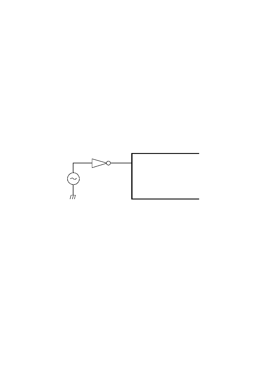
(3) Precautions for Use of External Clock
When an external clock is used, the signal should drive the X0 pin only, the X1 pin should be left open.
Figure 1.7.1 shows an example of an external clock connection.
Fig. 1.7.1 Example: Use of an External Clock
(4) Power Supply Pins
When there are multiple Vcc or Vss pins, semiconductor device design requires that in order to prevent
malfunctions such as latch-up, all internal elements of equivalent potential be connected. Also, to pre-
vent abnormal strobe signal operation due to unwanted lowering of emission or increases in ground
level, and to maintain standards for total output current, all elements must be connected to external
power supplies and grounds.
In addition it is recommended that Vcc and Vss of this device be connected with as little impedance as
possible from the current supply source.
It is further recommended that an approx. 0.1 F ceramic capacitor be placed near the device and con-
nected between the Vcc and Vss terminals as a bypass capacitor.
(5) Crystal Oscillator Circuits
Noise in the vicinity of the X0 and X1 pins can be a cause of abnormal operation in this device. Design-
ers should ensure that the X0 and X1 pins, and the crystal (or ceramic) oscillators as well as the bypass
capacitor to ground be placed as close together as possible, and that PC board wiring layouts provide as
little interference as possible from other wiring.
Also, PC board artwork can contribute toward stable of operation by surrounding the X0 and X1 pins
with ground. This is strongly recommended.
X1
X0
MB90242A/MB90V241
相關(guān)PDF資料 |
PDF描述 |
|---|---|
| MB90337PFM | 16-BIT, MROM, 24 MHz, MICROCONTROLLER, PQFP64 |
| MB90F337PFM | 16-BIT, FLASH, 24 MHz, MICROCONTROLLER, PQFP64 |
| MB90352SPFV | 16-BIT, FLASH, 24 MHz, MICROCONTROLLER, PQFP64 |
| MB90F352SPFV | 16-BIT, FLASH, 24 MHz, MICROCONTROLLER, PQFP64 |
| MB90F352PFV | 16-BIT, FLASH, 24 MHz, MICROCONTROLLER, PQFP64 |
相關(guān)代理商/技術(shù)參數(shù) |
參數(shù)描述 |
|---|---|
| MB90246 | 制造商:FUJITSU 制造商全稱:Fujitsu Component Limited. 功能描述:16-bit Proprietary Microcontroller |
| MB90246A | 制造商:FUJITSU 制造商全稱:Fujitsu Component Limited. 功能描述:16-bit Proprietary Microcontroller |
| MB90246APFV | 制造商:FUJITSU 制造商全稱:Fujitsu Component Limited. 功能描述:16-bit Proprietary Microcontroller |
| MB90330 | 制造商:FUJITSU 制造商全稱:Fujitsu Component Limited. 功能描述:16-bit Proprietary Microcontroller |
| MB90330A | 制造商:FUJITSU 制造商全稱:Fujitsu Component Limited. 功能描述:16-bit Microcontroller |
發(fā)布緊急采購,3分鐘左右您將得到回復(fù)。