- 您現(xiàn)在的位置:買賣IC網(wǎng) > PDF目錄1890 > AD5560JSVUZ-REEL (Analog Devices Inc)IC DPS PROGRAMABLE W/DAC 64TQFP PDF資料下載
參數(shù)資料
| 型號(hào): | AD5560JSVUZ-REEL |
| 廠商: | Analog Devices Inc |
| 文件頁(yè)數(shù): | 55/68頁(yè) |
| 文件大小: | 0K |
| 描述: | IC DPS PROGRAMABLE W/DAC 64TQFP |
| 設(shè)計(jì)資源: | Integrated Device Power Supply for PAD with Output Voltage Range 0 V to 25 V (CN0130) |
| 標(biāo)準(zhǔn)包裝: | 1,500 |
| 類型: | 電源 |
| 應(yīng)用: | 自動(dòng)測(cè)試設(shè)備 |
| 安裝類型: | 表面貼裝 |
| 封裝/外殼: | 64-TQFP 裸露焊盤 |
| 供應(yīng)商設(shè)備封裝: | 64-TQFP-EP(10x10) |
| 包裝: | 帶卷 (TR) |
第1頁(yè)第2頁(yè)第3頁(yè)第4頁(yè)第5頁(yè)第6頁(yè)第7頁(yè)第8頁(yè)第9頁(yè)第10頁(yè)第11頁(yè)第12頁(yè)第13頁(yè)第14頁(yè)第15頁(yè)第16頁(yè)第17頁(yè)第18頁(yè)第19頁(yè)第20頁(yè)第21頁(yè)第22頁(yè)第23頁(yè)第24頁(yè)第25頁(yè)第26頁(yè)第27頁(yè)第28頁(yè)第29頁(yè)第30頁(yè)第31頁(yè)第32頁(yè)第33頁(yè)第34頁(yè)第35頁(yè)第36頁(yè)第37頁(yè)第38頁(yè)第39頁(yè)第40頁(yè)第41頁(yè)第42頁(yè)第43頁(yè)第44頁(yè)第45頁(yè)第46頁(yè)第47頁(yè)第48頁(yè)第49頁(yè)第50頁(yè)第51頁(yè)第52頁(yè)第53頁(yè)第54頁(yè)當(dāng)前第55頁(yè)第56頁(yè)第57頁(yè)第58頁(yè)第59頁(yè)第60頁(yè)第61頁(yè)第62頁(yè)第63頁(yè)第64頁(yè)第65頁(yè)第66頁(yè)第67頁(yè)第68頁(yè)
Data Sheet
AD5560
Rev. D | Page 59 of 68
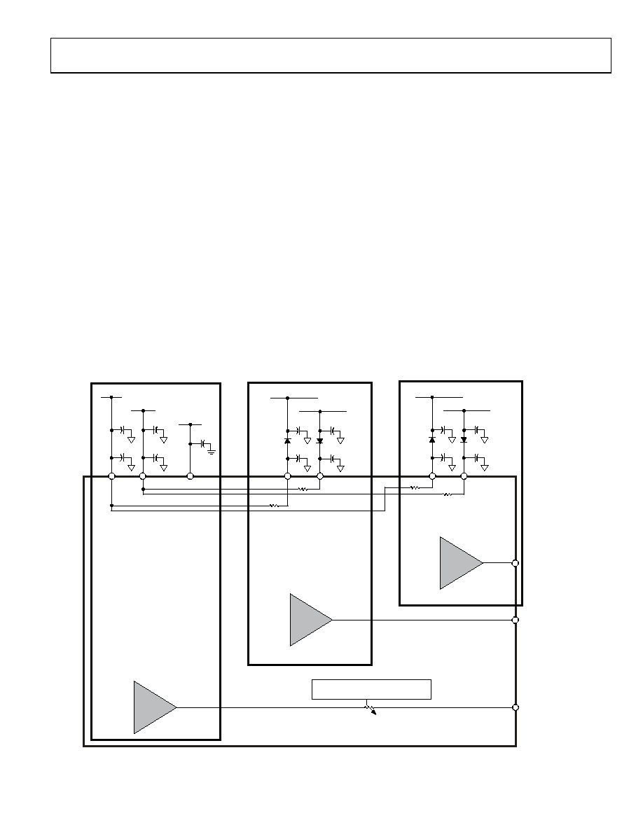
USING THE HCAVDDx AND HCAVSSx SUPPLIES
The first set of power supplies, AVDD and AVSS, provide power
to the DAC levels and associated circuitry. They also supply the
force amplifier stage for the low current ranges (ranges using
internal sense resistors up to 25 mA maximum).
The second set of power supplies, HCAVSS1 and HCAVDD1,
are intended to be used to minimize power consumption in
the AD5560 device for the EXTFORCE1 range (up to ±1.2 A).
Similarly, the HCAVSS2 and HCAVDD2 supplies are used for the
EXTFORCE2 range (up to ±500 mA). These supplies must be
less than or equal to the AVDD and AVSS supplies. When driving
high currents at low voltages, power can be greatly minimized
by ensuring that the supplies are at the lowest voltages.
Therefore, HCAVSSx and HCAVDDx can be switched externally
to different power rails as required by the set voltage range.
However, the design of the high current output stage means
that these supplies always have to be at a higher voltage than
the forced voltage, irrespective of the current range being used.
Therefore, depending on the level of supply switching, external
diodes may be required in series with each of the HCAVDDx
internal pull-up resistors between the supplies (see Figure 59).
Using diodes here allows a more flexible use of supplies and
can minimize the amount of supply switching required. In the
example, the AVDD and AVSS supplies can support the high
voltage needs, whereas the HCAVDDx and HCAVSSx supplies
support the low voltage, higher current ranges. Diode selection
should take into account the current carrying requirements.
Supply selection for HCAVDDx and HCAVSSx supplies must
allow for this extra voltage drop.
POWER SUPPLY SEQUENCING
When the supplies are connected to the AD5560, it is important
that the AGND and DGND pins be connected to the relevant
ground plane before the positive or negative supplies are applied.
In most applications, this is not an issue because the ground
pins for the power supplies are connected to the ground pins of
the AD5560 via ground planes. The AVDD and AVSS supplies
must be applied to the device either before or at the same time
There are no known supply sequences surrounding the DVCC
supply, although it is recommended that it be applied as
indicated by the absolute maximum ratings (see Table 3).
AD5560
33k
1200mA
RANGE
500mA
RANGE
FORCE
DUT RANGE
0V TO +25V
OUTPUT RANGE
0V TO +25V
INTERNAL RSENSE
±0.5V AT FULL CURRENT
INTERNAL RANGE SELECT
(5A, 25A, 250A, 2.5mA, 25mA)
EXTFORCE1
DUT RANGE
–2V TO +3V
EXTFORCE2
DUT RANGE
0V TO +6V
ALLOW ±0.5V
FOR EXT RSENSE
OUTPUT RANGE
–2.5V TO +3.5V
2. HIGHEST CURRENT
RANGE
1. LOW CURRENT,
HIGH VOLTAGE
3. MIDCURRENT
RANGE
OUTPUT RANGE
–0.2V TO +6.5V
ALLOW ±0.5V FOR EXT RSENSE
+
10F
+
0.1F
10F
0.1F
HCAVDD2 = +9V
HCAVSS2 = –5V
HCAVDD1 = +6V
HCAVSS1 = –5V
+
10F
+
0.1F
10F
0.1F
+
AVDD = +28V
AVSS = –5V
+
10F
+
0.1F
DVCC = 3V/5V
+
0.1F
10F
0.1F
+
33k
100k
07779-
012
Figure 59. Example of Using the Extra Supply Rails Within the AD5560 to Achieve Multiple Voltage/Current Ranges
相關(guān)PDF資料 |
PDF描述 |
|---|---|
| AD557JN | IC DAC 8BIT V-OUT 16-DIP |
| AD561KD | IC DAC 10BIT 5-15V IN MONO 16DIP |
| AD565AKD | IC DAC 12BIT MONO 250NS 24-CDIP |
| AD5663BCPZ-R2 | IC DAC NANO 16BIT DUAL 10-LFCSP |
| AD5678BRUZ-1 | IC DAC 12/16BIT SPI/SRL 14TSSOP |
相關(guān)代理商/技術(shù)參數(shù) |
參數(shù)描述 |
|---|---|
| AD5561JBCZ | 制造商:Analog Devices 功能描述: |
| AD5562ACPZ-R7 | 制造商:Analog Devices 功能描述: |
| AD5564B | 制造商:未知廠家 制造商全稱:未知廠家 功能描述:Industrial Control IC |
| AD557 | 制造商:AD 制造商全稱:Analog Devices 功能描述:a DACPORT Low Cost, Complete uP-Compatible 8-Bit DAC |
| AD557_01 | 制造商:AD 制造商全稱:Analog Devices 功能描述:a DACPORT Low Cost, Complete uP-Compatible 8-Bit DAC |
發(fā)布緊急采購(gòu),3分鐘左右您將得到回復(fù)。