- 您現(xiàn)在的位置:買賣IC網(wǎng) > PDF目錄360516 > 7544 3.3V LDO POSITVE VOLTAGE REGULATOR 2% TOL. PDF資料下載
參數(shù)資料
| 型號(hào): | 7544 |
| 英文描述: | 3.3V LDO POSITVE VOLTAGE REGULATOR 2% TOL. |
| 中文描述: | 7544Group數(shù)據(jù)表數(shù)據(jù)表503K/JUN.25.03 |
| 文件頁數(shù): | 26/54頁 |
| 文件大小: | 503K |
| 代理商: | 7544 |
第1頁第2頁第3頁第4頁第5頁第6頁第7頁第8頁第9頁第10頁第11頁第12頁第13頁第14頁第15頁第16頁第17頁第18頁第19頁第20頁第21頁第22頁第23頁第24頁第25頁當(dāng)前第26頁第27頁第28頁第29頁第30頁第31頁第32頁第33頁第34頁第35頁第36頁第37頁第38頁第39頁第40頁第41頁第42頁第43頁第44頁第45頁第46頁第47頁第48頁第49頁第50頁第51頁第52頁第53頁第54頁
Rev.1.02 2003.06.25 page 26 of 53
7544 Group
PRELIMINARY
Notice: This is not a final specification.
Some parametric limits are subject to change.
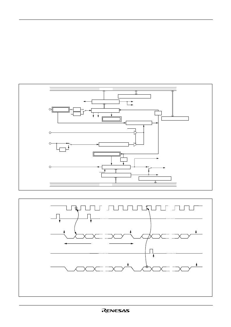
Fig. 28 Block diagram of UART serial I/O
(2) Asynchronous Serial I/O (UART) Mode
Clock asynchronous serial I/O mode (UART) can be selected by
clearing the serial I/O mode selection bit of the serial I/O control
register to
“
0
”
.
Eight serial data transfer formats can be selected, and the transfer
formats used by a transmitter and receiver must be identical.
The transmit and receive shift registers each have a buffer, but the
two buffers have the same address in memory. Since the shift reg-
ister cannot be written to or read from directly, transmit data is
written to the transmit buffer register, and receive data is read
from the receive buffer register.
The transmit buffer register can also hold the next data to be
transmitted, and the receive buffer register can hold a character
while the next character is being received.
Fig. 29 Operation of UART serial I/O function
X
IN
1/4
OE
PE FE
1/16
1/16
Data bus
Receive buffer register
Address 0018
16
Receive shift register
Receive buffer full flag (RBF)
Receive interrupt request (RI)
Baud rate generator
Address 001C
16
Frequency division ratio 1/(n+
1)
ST/SP/PA generator
Transmit buffer register
Data bus
Transmit shift register
Address
0018
16
Transmit shift completion flag (TSC)
Transmit buffer empty flag (TBE)
Address
0019
16
Serial I/O status register
Transmit interrupt request (TI)
ST detector
SP detector
UART control register
Address 001B
16
Character length selection bit
Address 001A
16
BRG count source selection bit
Transmit interrupt source selection bit
Serial I/O synchronous clock selection bit
Clock control circuit
Character length selection bit
7 bits
8 bits
Serial I/O control register
P1
2
/S
CLK
P1
0
/R
X
D
P1
1
/T
X
D
TSC=0
TBE=1
RBF=0
TBE=0
TBE=0
RBF=1
RBF=1
ST
D
0
D
1
SP
D
0
D
1
ST
SP
TBE=1
TSC=1
ST
D
0
D
1
SP
D
0
D
1
ST
SP
Transmit or receive clock
Transmit buffer write
signal
Generated at 2nd bit in 2-stop-bit mode
1 start bit
7 or 8 data bit
1 or 0 parity bit
1 or 2 stop bit (s)
1:
Error flag detection occurs at the same time that the RBF flag becomes
“
1
”
(at 1st stop bit, during reception).
2:
As the transmit interrupt (TI), when either the TBE or TSC flag becomes
“
1,
”
can be selected to occur depending on the setting of the transmit
interrupt source selection bit (TIC) of the serial I/O control register.
3:
The receive interrupt (RI) is set when the RBF flag becomes
“
1.
”
4:
After data is written to the transmit buffer when TSC=1, 0.5 to 1.5 cycles of the data shift cycle is necessary until changing to TSC=0.
Notes
Serial output T
X
D
Serial input R
X
D
Receive buffer read
signal
相關(guān)PDF資料 |
PDF描述 |
|---|---|
| 75450PC | Peripheral IC |
| D122D | Converter IC |
| D347D | Logic IC |
| D348D | Logic IC |
| 7545ARPDS-2 | HIGH VOLTAGE, LOW QUIESCENT CURRENT LDO, -40C to +125C, 3-SOT-89, T/R |
相關(guān)代理商/技術(shù)參數(shù) |
參數(shù)描述 |
|---|---|
| 754-4.47M | 制造商:OSCILENT 制造商全稱:Oscilent Corporation 功能描述:Ceramic Trap Double/Triple Peak |
| 754-4.6M | 制造商:OSCILENT 制造商全稱:Oscilent Corporation 功能描述:Ceramic Trap Double/Triple Peak |
| 754-4007-0 | 制造商:ROCK 功能描述: |
| 75-440-6 | 制造商:ATM 制造商全稱:ATM 功能描述:STANDARD GAIN HORN |
| 75-440-X | 制造商:ATM 制造商全稱:ATM 功能描述:HORN MOUNT APPLICATIONS |
發(fā)布緊急采購,3分鐘左右您將得到回復(fù)。