- 您現(xiàn)在的位置:買賣IC網(wǎng) > PDF目錄359352 > VCT3801A (MICRONAS SEMICONDUCTOR HOLDING AG) Video/Controller/Teletext IC Family PDF資料下載
參數(shù)資料
| 型號(hào): | VCT3801A |
| 廠商: | MICRONAS SEMICONDUCTOR HOLDING AG |
| 英文描述: | Video/Controller/Teletext IC Family |
| 中文描述: | 視頻/控制/圖文電視IC系列 |
| 文件頁(yè)數(shù): | 32/172頁(yè) |
| 文件大小: | 2243K |
| 代理商: | VCT3801A |
第1頁(yè)第2頁(yè)第3頁(yè)第4頁(yè)第5頁(yè)第6頁(yè)第7頁(yè)第8頁(yè)第9頁(yè)第10頁(yè)第11頁(yè)第12頁(yè)第13頁(yè)第14頁(yè)第15頁(yè)第16頁(yè)第17頁(yè)第18頁(yè)第19頁(yè)第20頁(yè)第21頁(yè)第22頁(yè)第23頁(yè)第24頁(yè)第25頁(yè)第26頁(yè)第27頁(yè)第28頁(yè)第29頁(yè)第30頁(yè)第31頁(yè)當(dāng)前第32頁(yè)第33頁(yè)第34頁(yè)第35頁(yè)第36頁(yè)第37頁(yè)第38頁(yè)第39頁(yè)第40頁(yè)第41頁(yè)第42頁(yè)第43頁(yè)第44頁(yè)第45頁(yè)第46頁(yè)第47頁(yè)第48頁(yè)第49頁(yè)第50頁(yè)第51頁(yè)第52頁(yè)第53頁(yè)第54頁(yè)第55頁(yè)第56頁(yè)第57頁(yè)第58頁(yè)第59頁(yè)第60頁(yè)第61頁(yè)第62頁(yè)第63頁(yè)第64頁(yè)第65頁(yè)第66頁(yè)第67頁(yè)第68頁(yè)第69頁(yè)第70頁(yè)第71頁(yè)第72頁(yè)第73頁(yè)第74頁(yè)第75頁(yè)第76頁(yè)第77頁(yè)第78頁(yè)第79頁(yè)第80頁(yè)第81頁(yè)第82頁(yè)第83頁(yè)第84頁(yè)第85頁(yè)第86頁(yè)第87頁(yè)第88頁(yè)第89頁(yè)第90頁(yè)第91頁(yè)第92頁(yè)第93頁(yè)第94頁(yè)第95頁(yè)第96頁(yè)第97頁(yè)第98頁(yè)第99頁(yè)第100頁(yè)第101頁(yè)第102頁(yè)第103頁(yè)第104頁(yè)第105頁(yè)第106頁(yè)第107頁(yè)第108頁(yè)第109頁(yè)第110頁(yè)第111頁(yè)第112頁(yè)第113頁(yè)第114頁(yè)第115頁(yè)第116頁(yè)第117頁(yè)第118頁(yè)第119頁(yè)第120頁(yè)第121頁(yè)第122頁(yè)第123頁(yè)第124頁(yè)第125頁(yè)第126頁(yè)第127頁(yè)第128頁(yè)第129頁(yè)第130頁(yè)第131頁(yè)第132頁(yè)第133頁(yè)第134頁(yè)第135頁(yè)第136頁(yè)第137頁(yè)第138頁(yè)第139頁(yè)第140頁(yè)第141頁(yè)第142頁(yè)第143頁(yè)第144頁(yè)第145頁(yè)第146頁(yè)第147頁(yè)第148頁(yè)第149頁(yè)第150頁(yè)第151頁(yè)第152頁(yè)第153頁(yè)第154頁(yè)第155頁(yè)第156頁(yè)第157頁(yè)第158頁(yè)第159頁(yè)第160頁(yè)第161頁(yè)第162頁(yè)第163頁(yè)第164頁(yè)第165頁(yè)第166頁(yè)第167頁(yè)第168頁(yè)第169頁(yè)第170頁(yè)第171頁(yè)第172頁(yè)
VCT 38xxA
ADVANCE INFORMATION
32
Micronas
2.15.I
2
C Bus Slave Interface
Communication between the VDP and the TV control-
ler is done via I
2
C bus. For detailed information on the
I
2
C bus please refer to the Philips manual ‘I
2
C bus
Specification’.
The VDP has two I
2
C bus slave interfaces (for compat-
ibility with VPC/DDP applications)
one in the
front-end and one in the back-end. Both I
2
C bus inter-
faces use I
2
C clock synchronization to slow down the
interface if required. Both I
2
C bus interfaces use one
level of subaddress: the I
2
C bus chip address is used
to address the VDP and a subaddress selects one of
the internal registers. The I
2
C bus chip addresses are
given below:
The registers of the VDP have 8 or 16-bit data size;
16-bit registers are accessed by reading/writing two
8-bit data words.
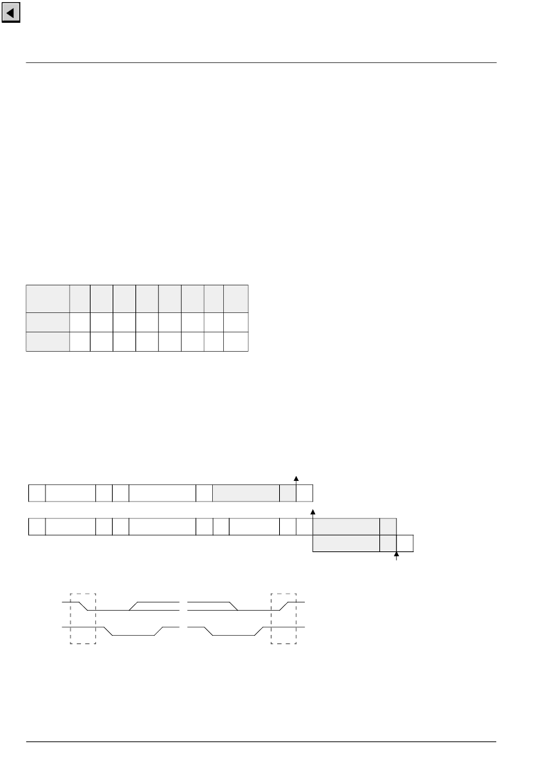
Fig. 2–26 shows I
2
C bus protocols for read and write
operations of the interface; the read operation requires
an extra start condition and repetition of the chip
address with read command set.
2.15.1.Control and Status Registers
Table 2–3 gives definitions of the VDP control and sta-
tus registers. The number of bits indicated for each
register in the table is the number of bits implemented
in hardware, i.e. a 9-bit register must always be
accessed using two data bytes but the 7 MSB will be
‘don’t care’ on write operations and ‘0’ on read opera-
tions. Write registers that can be read back are indi-
cated in Table 2–3.
Functions implemented by software in the on-chip con-
trol microprocessor (FP) are explained in Table 2–5.
A hardware reset initializes all control registers to 0.
The automatic chip initialization loads a selected set of
registers with the default values given in Table 2–3.
The register modes given in Table 2–3 are
– w:
write only register
– w/r:
write/read data register
– r:
read data from VDP
– v:
register is latched with vertical sync
– h:
register is latched with horizontal
Fig. 2–26:
I
2
C bus protocols
Table 2–2:
I
2
C chip addresses
Chip
Address
A6
A5
A4
A3
A2
A1
A0
R/W
front-end
1
0
0
0
1
1
1
1/0
back-end
1
0
0
0
1
0
1
1/0
P
S
1
0
SDA
SCL
S
S
1000 111
1000 111
W Ack
Ack
W
0111 1100
0111 1100
Ack
Ack
S
1 or 2 byte Data
1000 111
R
high byte Data
low byte Data
P
W
R
Ack
Nak
S
P
=
=
=
=
=
=
0
1
0
1
Start
Stop
Ack
Nak P
I
2
C write access
subaddress 7c
I
2
C read access
subaddress 7c
相關(guān)PDF資料 |
PDF描述 |
|---|---|
| VCU2133 | High-Speed coder/decoder IC |
| VCX2150A | Surface mount 15.88 mm SQ (.625 SQ) |
| VCX2154A | Surface mount 15.88 mm SQ (.625 SQ) |
| VCXO-105N | VCXO |
| VCXO-199 | VCXO |
相關(guān)代理商/技術(shù)參數(shù) |
參數(shù)描述 |
|---|---|
| VCT3802A | 制造商:MICRONAS 制造商全稱:MICRONAS 功能描述:Video/Controller/Teletext IC Family |
| VCT3803A | 制造商:MICRONAS 制造商全稱:MICRONAS 功能描述:Video/Controller/Teletext IC Family |
| VCT3804A | 制造商:MICRONAS 制造商全稱:MICRONAS 功能描述:Video/Controller/Teletext IC Family |
| VCT3811A | 制造商:MICRONAS 制造商全稱:MICRONAS 功能描述:Video/Controller/Teletext IC Family |
| VCT3831A | 制造商:MICRONAS 制造商全稱:MICRONAS 功能描述:Video/Controller/Teletext IC Family |
發(fā)布緊急采購(gòu),3分鐘左右您將得到回復(fù)。