- 您現(xiàn)在的位置:買賣IC網(wǎng) > PDF目錄192306 > S71PL191HB0BFI100 (SPANSION LLC) SPECIALTY MEMORY CIRCUIT, PBGA73 PDF資料下載
參數(shù)資料
| 型號(hào): | S71PL191HB0BFI100 |
| 廠商: | SPANSION LLC |
| 元件分類: | 存儲(chǔ)器 |
| 英文描述: | SPECIALTY MEMORY CIRCUIT, PBGA73 |
| 封裝: | 9 X 13 MM, LEAD FREE, FBGA-73 |
| 文件頁(yè)數(shù): | 171/172頁(yè) |
| 文件大小: | 4662K |
| 代理商: | S71PL191HB0BFI100 |
第1頁(yè)第2頁(yè)第3頁(yè)第4頁(yè)第5頁(yè)第6頁(yè)第7頁(yè)第8頁(yè)第9頁(yè)第10頁(yè)第11頁(yè)第12頁(yè)第13頁(yè)第14頁(yè)第15頁(yè)第16頁(yè)第17頁(yè)第18頁(yè)第19頁(yè)第20頁(yè)第21頁(yè)第22頁(yè)第23頁(yè)第24頁(yè)第25頁(yè)第26頁(yè)第27頁(yè)第28頁(yè)第29頁(yè)第30頁(yè)第31頁(yè)第32頁(yè)第33頁(yè)第34頁(yè)第35頁(yè)第36頁(yè)第37頁(yè)第38頁(yè)第39頁(yè)第40頁(yè)第41頁(yè)第42頁(yè)第43頁(yè)第44頁(yè)第45頁(yè)第46頁(yè)第47頁(yè)第48頁(yè)第49頁(yè)第50頁(yè)第51頁(yè)第52頁(yè)第53頁(yè)第54頁(yè)第55頁(yè)第56頁(yè)第57頁(yè)第58頁(yè)第59頁(yè)第60頁(yè)第61頁(yè)第62頁(yè)第63頁(yè)第64頁(yè)第65頁(yè)第66頁(yè)第67頁(yè)第68頁(yè)第69頁(yè)第70頁(yè)第71頁(yè)第72頁(yè)第73頁(yè)第74頁(yè)第75頁(yè)第76頁(yè)第77頁(yè)第78頁(yè)第79頁(yè)第80頁(yè)第81頁(yè)第82頁(yè)第83頁(yè)第84頁(yè)第85頁(yè)第86頁(yè)第87頁(yè)第88頁(yè)第89頁(yè)第90頁(yè)第91頁(yè)第92頁(yè)第93頁(yè)第94頁(yè)第95頁(yè)第96頁(yè)第97頁(yè)第98頁(yè)第99頁(yè)第100頁(yè)第101頁(yè)第102頁(yè)第103頁(yè)第104頁(yè)第105頁(yè)第106頁(yè)第107頁(yè)第108頁(yè)第109頁(yè)第110頁(yè)第111頁(yè)第112頁(yè)第113頁(yè)第114頁(yè)第115頁(yè)第116頁(yè)第117頁(yè)第118頁(yè)第119頁(yè)第120頁(yè)第121頁(yè)第122頁(yè)第123頁(yè)第124頁(yè)第125頁(yè)第126頁(yè)第127頁(yè)第128頁(yè)第129頁(yè)第130頁(yè)第131頁(yè)第132頁(yè)第133頁(yè)第134頁(yè)第135頁(yè)第136頁(yè)第137頁(yè)第138頁(yè)第139頁(yè)第140頁(yè)第141頁(yè)第142頁(yè)第143頁(yè)第144頁(yè)第145頁(yè)第146頁(yè)第147頁(yè)第148頁(yè)第149頁(yè)第150頁(yè)第151頁(yè)第152頁(yè)第153頁(yè)第154頁(yè)第155頁(yè)第156頁(yè)第157頁(yè)第158頁(yè)第159頁(yè)第160頁(yè)第161頁(yè)第162頁(yè)第163頁(yè)第164頁(yè)第165頁(yè)第166頁(yè)第167頁(yè)第168頁(yè)第169頁(yè)第170頁(yè)當(dāng)前第171頁(yè)第172頁(yè)

2S29JL064H
S29JL064HA1 May 7, 2004
Pr el i m i n ary
General Description
The S29JL064H is a 64 megabit, 3.0 volt-only flash memory device, organized as
4,194,304 words of 16 bits each or 8,388,608 bytes of 8 bits each. Word mode
Data appears on DQ15–DQ0; byte mode data appears on DQ7–DQ0. The device
is designed to be programmed in-system with the standard 3.0 volt VCC supply,
and can also be programmed in standard EPROM programmers.
Standard control pins—chip enable (CE#), write enable (WE#), and output en-
able (OE#)—control normal read and write operations, and avoid bus contention
issues.
The device requires only a single 3.0 volt power supply for both read and write
functions. Internally generated and regulated voltages are provided for the pro-
gram and erase operations.
Simultaneous Read/Write Operations with Zero Latency
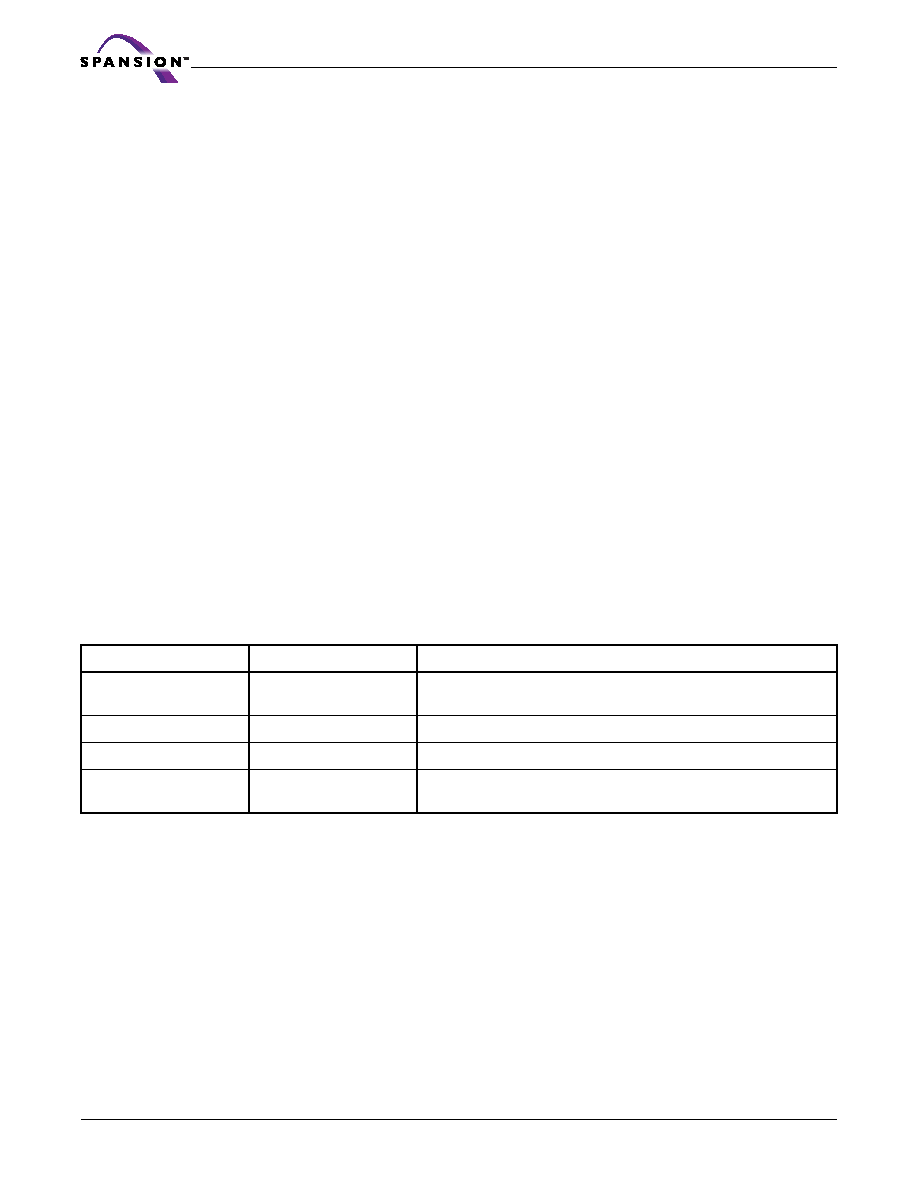
The Simultaneous Read/Write architecture provides simultaneous operation
by dividing the memory space into four banks, two 8 Mb banks with small and
large sectors, and two 24 Mb banks of large sectors. Sector addresses are fixed,
system software can be used to form user-defined bank groups.
During an Erase/Program operation, any of the three non-busy banks may be
read from. Note that only two banks can operate simultaneously. The device can
improve overall system performance by allowing a host system to program or
erase in one bank, then immediately and simultaneously read from the other
bank, with zero latency. This releases the system from waiting for the completion
of program or erase operations.
The S29JL064H can be organized as both a top and bottom boot sector
configuration.
S29JL064H Features
The SecSi (Secured Silicon) Sector is an extra 256 byte sector capable of
being permanently locked by FASL or customers. [The SecSi Customer Indicator
Bit (DQ6) is permanently set to 1 if the part has been customer locked and per-
manently set to 0 if the part has been factory locked.] This way, customer
lockable parts can never be used to replace a factory locked part.
Factory locked parts provide several options. The SecSi Sector may store a se-
cure, random 16 byte ESN (Electronic Serial Number), customer code
(programmed through Spansion programming services), or both. Customer Lock-
able parts may utilize the SecSi Sector as bonus space, reading and writing like
any other flash sector, or may permanently lock their own code there.
DMS (Data Management Software) allows systems to easily take advantage
of the advanced architecture of the simultaneous read/write product line by al-
Bank
Megabits
Sector Sizes
Bank 1
8 Mb
Eight 8 Kbyte/4 Kword,
Fifteen 64 Kbyte/32 Kword
Bank 2
24 Mb
Forty-eight 64 Kbyte/32 Kword
Bank 3
24 Mb
Forty-eight 64 Kbyte/32 Kword
Bank 4
8 Mb
Eight 8 Kbyte/4 Kword,
Fifteen 64 Kbyte/32 Kword
相關(guān)PDF資料 |
PDF描述 |
|---|---|
| S71VS128RC0ZHK203 | SPECIALTY MEMORY CIRCUIT, PBGA56 |
| S71VS128RC0ZHK2L2 | SPECIALTY MEMORY CIRCUIT, PBGA56 |
| S71WS512ND0BAWEH | SPECIALTY MEMORY CIRCUIT, PBGA84 |
| S72NS512PE0AHGL02 | SPECIALTY MEMORY CIRCUIT, PBGA133 |
| S7911 | PIN PHOTO DIODE |
相關(guān)代理商/技術(shù)參數(shù) |
參數(shù)描述 |
|---|---|
| S71PL254 | 制造商:SPANSION 制造商全稱:SPANSION 功能描述:STACKED MULTI CHIP PRODUCT FLASH MEMORY AND RAM |
| S71PL254J | 制造商:SPANSION 制造商全稱:SPANSION 功能描述:STACKED MULTI CHIP PRODUCT FLASH MEMORY AND RAM |
| S71PL254J04BAW0Z0 | 制造商:SPANSION 制造商全稱:SPANSION 功能描述:Based MCPs |
| S71PL254J04BAW0Z2 | 制造商:SPANSION 制造商全稱:SPANSION 功能描述:Based MCPs |
| S71PL254J04BAW0Z3 | 制造商:SPANSION 制造商全稱:SPANSION 功能描述:Based MCPs |
發(fā)布緊急采購(gòu),3分鐘左右您將得到回復(fù)。