- 您現(xiàn)在的位置:買賣IC網(wǎng) > PDF目錄192306 > S71PL191HB0BFI100 (SPANSION LLC) SPECIALTY MEMORY CIRCUIT, PBGA73 PDF資料下載
參數(shù)資料
| 型號: | S71PL191HB0BFI100 |
| 廠商: | SPANSION LLC |
| 元件分類: | 存儲器 |
| 英文描述: | SPECIALTY MEMORY CIRCUIT, PBGA73 |
| 封裝: | 9 X 13 MM, LEAD FREE, FBGA-73 |
| 文件頁數(shù): | 127/172頁 |
| 文件大?。?/td> | 4662K |
| 代理商: | S71PL191HB0BFI100 |
第1頁第2頁第3頁第4頁第5頁第6頁第7頁第8頁第9頁第10頁第11頁第12頁第13頁第14頁第15頁第16頁第17頁第18頁第19頁第20頁第21頁第22頁第23頁第24頁第25頁第26頁第27頁第28頁第29頁第30頁第31頁第32頁第33頁第34頁第35頁第36頁第37頁第38頁第39頁第40頁第41頁第42頁第43頁第44頁第45頁第46頁第47頁第48頁第49頁第50頁第51頁第52頁第53頁第54頁第55頁第56頁第57頁第58頁第59頁第60頁第61頁第62頁第63頁第64頁第65頁第66頁第67頁第68頁第69頁第70頁第71頁第72頁第73頁第74頁第75頁第76頁第77頁第78頁第79頁第80頁第81頁第82頁第83頁第84頁第85頁第86頁第87頁第88頁第89頁第90頁第91頁第92頁第93頁第94頁第95頁第96頁第97頁第98頁第99頁第100頁第101頁第102頁第103頁第104頁第105頁第106頁第107頁第108頁第109頁第110頁第111頁第112頁第113頁第114頁第115頁第116頁第117頁第118頁第119頁第120頁第121頁第122頁第123頁第124頁第125頁第126頁當(dāng)前第127頁第128頁第129頁第130頁第131頁第132頁第133頁第134頁第135頁第136頁第137頁第138頁第139頁第140頁第141頁第142頁第143頁第144頁第145頁第146頁第147頁第148頁第149頁第150頁第151頁第152頁第153頁第154頁第155頁第156頁第157頁第158頁第159頁第160頁第161頁第162頁第163頁第164頁第165頁第166頁第167頁第168頁第169頁第170頁第171頁第172頁
42
S29PL127H/S29PL129H
S29PL127H_129H_00A1 May 7, 2004
Pr el i m i n ary
Write Pulse “Glitch” Protection
Noise pulses of less than 3 ns (typical) on OE#, CE#, or WE# do not initiate a
write cycle.
Logical Inhibit
Write cycles are inhibited by holding any one of OE# = VIL, CE# = VIH or WE# =
VIH. To initiate a write cycle, CE# and WE# must be a logical zero while OE# is a
logical one.
Power-Up Write Inhibit
If WE# = CE# = VIL and OE# = VIH during power up, the device does not accept
commands on the rising edge of WE#. The internal state machine is automatically
reset to the read mode on power-up.
COMMON FLASH MEMORY INTERFACE (CFI)
The Common Flash Interface (CFI) specification outlines device and host system
software interrogation handshake, which allows specific vendor-specified soft-
ware algorithms to be used for entire families of devices. Software support can
then be device-independent, JEDEC ID-independent, and forward- and back-
ward-compatible for the specified flash device families. Flash vendors can
standardize their existing interfaces for long-term compatibility.
This device enters the CFI Query mode when the system writes the CFI Query
command, 98h, to address 55h, any time the device is ready to read array data.
terminate reading CFI data, the system must write the reset command. The CFI
Query mode is not accessible when the device is executing an Embedded Program
or embedded Erase algorithm.
The system can also write the CFI query command when the device is in the au-
toselect mode. The device enters the CFI query mode, and the system can read
command to return the device to reading array data.
For further information, please refer to the CFI Specification and CFI Publication
100, at http://www.amd.com/flash/cfi. Contact your local sales office for copies
of these documents.
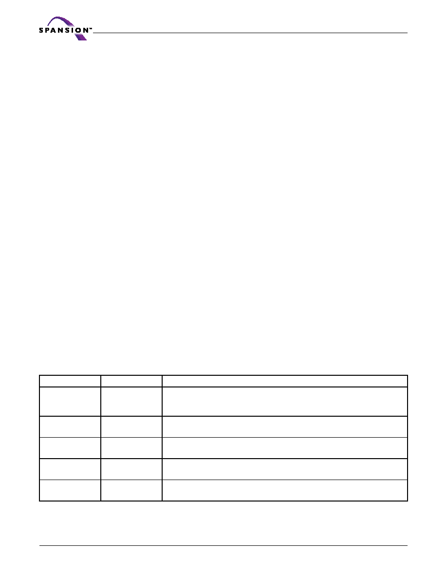
Table 12. CFI Query Identification String
Addresses
Data
Description
10h
11h
12h
0051h
0052h
0059h
Query Unique ASCII string “QRY”
13h
14h
0002h
0000h
Primary OEM Command Set
15h
16h
0040h
0000h
Address for Primary Extended Table
17h
18h
0000h
Alternate OEM Command Set (00h = none exists)
19h
1Ah
0000h
Address for Alternate OEM Extended Table (00h = none exists)
相關(guān)PDF資料 |
PDF描述 |
|---|---|
| S71VS128RC0ZHK203 | SPECIALTY MEMORY CIRCUIT, PBGA56 |
| S71VS128RC0ZHK2L2 | SPECIALTY MEMORY CIRCUIT, PBGA56 |
| S71WS512ND0BAWEH | SPECIALTY MEMORY CIRCUIT, PBGA84 |
| S72NS512PE0AHGL02 | SPECIALTY MEMORY CIRCUIT, PBGA133 |
| S7911 | PIN PHOTO DIODE |
相關(guān)代理商/技術(shù)參數(shù) |
參數(shù)描述 |
|---|---|
| S71PL254 | 制造商:SPANSION 制造商全稱:SPANSION 功能描述:STACKED MULTI CHIP PRODUCT FLASH MEMORY AND RAM |
| S71PL254J | 制造商:SPANSION 制造商全稱:SPANSION 功能描述:STACKED MULTI CHIP PRODUCT FLASH MEMORY AND RAM |
| S71PL254J04BAW0Z0 | 制造商:SPANSION 制造商全稱:SPANSION 功能描述:Based MCPs |
| S71PL254J04BAW0Z2 | 制造商:SPANSION 制造商全稱:SPANSION 功能描述:Based MCPs |
| S71PL254J04BAW0Z3 | 制造商:SPANSION 制造商全稱:SPANSION 功能描述:Based MCPs |
發(fā)布緊急采購,3分鐘左右您將得到回復(fù)。