- 您現(xiàn)在的位置:買賣IC網(wǎng) > PDF目錄368020 > PI7C21P100NH (Pericom Semiconductor Corp.) 2-PORT PCI-X BRIDGE PDF資料下載
參數(shù)資料
| 型號(hào): | PI7C21P100NH |
| 廠商: | Pericom Semiconductor Corp. |
| 英文描述: | 2-PORT PCI-X BRIDGE |
| 中文描述: | 2端口PCI - X橋接 |
| 文件頁(yè)數(shù): | 66/77頁(yè) |
| 文件大小: | 603K |
| 代理商: | PI7C21P100NH |
第1頁(yè)第2頁(yè)第3頁(yè)第4頁(yè)第5頁(yè)第6頁(yè)第7頁(yè)第8頁(yè)第9頁(yè)第10頁(yè)第11頁(yè)第12頁(yè)第13頁(yè)第14頁(yè)第15頁(yè)第16頁(yè)第17頁(yè)第18頁(yè)第19頁(yè)第20頁(yè)第21頁(yè)第22頁(yè)第23頁(yè)第24頁(yè)第25頁(yè)第26頁(yè)第27頁(yè)第28頁(yè)第29頁(yè)第30頁(yè)第31頁(yè)第32頁(yè)第33頁(yè)第34頁(yè)第35頁(yè)第36頁(yè)第37頁(yè)第38頁(yè)第39頁(yè)第40頁(yè)第41頁(yè)第42頁(yè)第43頁(yè)第44頁(yè)第45頁(yè)第46頁(yè)第47頁(yè)第48頁(yè)第49頁(yè)第50頁(yè)第51頁(yè)第52頁(yè)第53頁(yè)第54頁(yè)第55頁(yè)第56頁(yè)第57頁(yè)第58頁(yè)第59頁(yè)第60頁(yè)第61頁(yè)第62頁(yè)第63頁(yè)第64頁(yè)第65頁(yè)當(dāng)前第66頁(yè)第67頁(yè)第68頁(yè)第69頁(yè)第70頁(yè)第71頁(yè)第72頁(yè)第73頁(yè)第74頁(yè)第75頁(yè)第76頁(yè)第77頁(yè)
PI7C21P100
2-PORT PCI-X BRIDGE
ADVANCE INFORMATION
Page 66 of 77
June 10, 2005 Revision 1.06
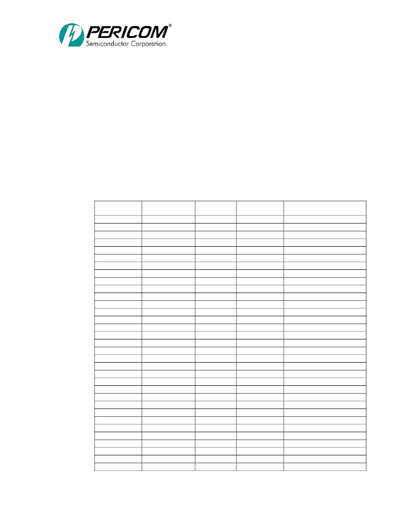
9.4
BOUNDARY SCAN REGISTER
The boundary scan register is a required set of serial-shiftable register cells, formed by
connecting boundary scan cells placed at the device’s signal pins into a shift register path. The
VDD, VSS, and JTAG pins are NOT in the boundary-scan chain. The input to the shift
register is TDI and the output from the shift register is TDO. There are 4 different types of
boundary scan cells, based on the function of each signal pin.
The boundary scan register cells are dedicated logic and do not have any system function.
Data may be loaded into the boundary-scan register master cells from the device input pins
and output pin-drivers in parallel by the mandatory SAMPLE and EXTEST instructions.
Parallel loading takes place on the rising edge of TCK.
9.5
JTAG BOUNDARY REGISTER ORDER
Table 9-1 JTAG BOUNDARY SCAN REGISTER
Boundary Scan
Register Number
0
1
2
3
4
5
6
7
8
9
10
11
12
13
14
15
16
17
18
19
20
21
22
23
24
25
26
27
28
29
30
31
32
Pin Name
P_ACK64#
P_AD[0]
P_AD[1]
P_AD[2]
P_AD[3]
P_AD[4]
P_AD[5]
P_AD[6]
P_AD[7]
P_AD[8]
P_AD[9]
P_AD[10]
P_AD[11]
P_AD[12]
P_AD[13]
P_AD[14]
P_AD[15]
P_AD[16]
P_AD[17]
P_AD[18]
P_AD[19]
P_AD[20]
P_AD[21]
P_AD[22]
P_AD[23]
P_AD[24]
P_AD[25]
P_AD[26]
P_AD[27]
P_AD[28]
P_AD[29]
P_AD[30]
P_AD[31]
Ball Location
A2
B13
C13
B14
C15
A19
B16
C16
A20
B17
C17
C19
D18
F22
F20
G22
B20
G21
H22
H21
J22
J21
K22
D23
K21
E23
K20
G23
L22
L21
M22
M21
J23
Type
BIDIR
BIDIR
BIDIR
BIDIR
BIDIR
BIDIR
BIDIR
BIDIR
BIDIR
BIDIR
BIDIR
BIDIR
BIDIR
BIDIR
BIDIR
BIDIR
BIDIR
BIDIR
BIDIR
BIDIR
BIDIR
BIDIR
BIDIR
BIDIR
BIDIR
BIDIR
BIDIR
BIDIR
BIDIR
BIDIR
BIDIR
BIDIR
BIDIR
Tri-state Control Cell
208
209
210
211
212
213
214
215
216
217
218
219
220
221
222
223
224
225
226
227
228
229
230
231
232
233
234
235
236
237
238
239
240
相關(guān)PDF資料 |
PDF描述 |
|---|---|
| PI7C7100BNA | PCI Bus Interface/Controller |
| PI7C7100 | 3-Port PCI Bridge |
| PI7C7100CNA | 3-Port PCI Bridge |
| PI7C7300 | 3-PORT PCI-to-PCI BRIDGE |
| PI7C7300A | 3-PORT PCI-to-PCI BRIDGE |
相關(guān)代理商/技術(shù)參數(shù) |
參數(shù)描述 |
|---|---|
| PI7C21P100NHE | 功能描述:外圍驅(qū)動(dòng)器與原件 - PCI 3 Port PCI Bridge RoHS:否 制造商:PLX Technology 工作電源電壓: 最大工作溫度: 安裝風(fēng)格:SMD/SMT 封裝 / 箱體:FCBGA-1156 封裝:Tray |
| PI7C4025TRF4 | 制造商:Pericom Semiconductor Corporation 功能描述: |
| PI7C7100 | 制造商:PERICOM 制造商全稱:Pericom Semiconductor Corporation 功能描述:3-Port PCI Bridge |
| PI7C7100BNA | 制造商:Pericom Semiconductor Corporation 功能描述:3 PORT PCI TO PCI |
| PI7C7100CNA | 制造商:PERICOM 制造商全稱:Pericom Semiconductor Corporation 功能描述:3-Port PCI Bridge |
發(fā)布緊急采購(gòu),3分鐘左右您將得到回復(fù)。