- 您現(xiàn)在的位置:買賣IC網(wǎng) > PDF目錄369993 > pentium processor with MMX (Intel Corp.) 32-bit processor with MMX technology(32位帶MMX技術(shù)處理器) PDF資料下載
參數(shù)資料
| 型號: | pentium processor with MMX |
| 廠商: | Intel Corp. |
| 英文描述: | 32-bit processor with MMX technology(32位帶MMX技術(shù)處理器) |
| 中文描述: | 32位MMX技術(shù)(32位帶MMX公司的技術(shù)處理器處理器) |
| 文件頁數(shù): | 40/51頁 |
| 文件大小: | 479K |
| 代理商: | PENTIUM PROCESSOR WITH MMX |
第1頁第2頁第3頁第4頁第5頁第6頁第7頁第8頁第9頁第10頁第11頁第12頁第13頁第14頁第15頁第16頁第17頁第18頁第19頁第20頁第21頁第22頁第23頁第24頁第25頁第26頁第27頁第28頁第29頁第30頁第31頁第32頁第33頁第34頁第35頁第36頁第37頁第38頁第39頁當(dāng)前第40頁第41頁第42頁第43頁第44頁第45頁第46頁第47頁第48頁第49頁第50頁第51頁

PENTIUM PROCESSOR WITH MMX TECHNOLOGY
E
40
5/23/97 10:47 AM 24318502.DOC
11. This is a flight time specification, that includes both flight time and clock skew. The flight time is the time from where the
unloaded driver crosses 1.5V (50% of min V
), to where the receiver crosses the 1.5V level (50% of min V
CC
). See
Figure 11. The minimum flight time minus the clock skew must be greater than zero.
12.
Setup time is required to guarantee recognition on a specific clock. Pentium processor with MMX technology must meet
this specification for dual processor operation for the FLUSH# and RESET signals.
13. Hold time is required to guarantee recognition on a specific clock. Pentium processor with MMX technology must meet this
specification for dual processor operation for the FLUSH# and RESET signals.
14. All TTL timings are referenced from 1.5V.
15. To guarantee proper asynchronous recognition, the signal must have been de-asserted (inactive) for a minimum of two
clocks before being returned active and must meet the minimum pulse width.
16. This input may be driven asynchronously. However, when operating two processors in dual processing mode, FLUSH#
and RESET must be asserted synchronously to both processors.
17. When driven asynchronously, RESET, NMI, FLUSH#, R/S#, INIT and SMI# must be de-asserted (inactive) for a minimum
of two clocks before being returned active.
18. Timings are valid only when dual processor is present.
19. Maximum time DPEN# is valid from rising edge of RESET.
20. Minimum time DPEN# is valid after falling edge of RESET.
21. The D/C#, M/IO#, W/R#, CACHE# and A5–A31 signals are sampled only on the CLK that ADS# is active.
22. In order to override the internal defaults and guarantee that the BF[1:0] inputs remain stable while RESET is active, these
pins should be strapped directly to or through a pull-up/pull-down resistor to V
or ground. Driving these pins with active
logic is not recommended unless stability duringt RESET can be guaranteed. Similarly, CPUTYP should also be strapped
directly to or through a pull-up/pull-down resistor to V
CC3
or ground.
23. RESET is synchronous in dual processing mode. All signals which have a setup or hold time with respect to a falling or
rising edge of RESET in UP mode, should be measured with respect to the first processor clock edge in which RESET is
sampled either active or inactive in dual processing mode.
24. The PHIT# and PHITM# signals operate at the core frequency.
25. These signals are measured on the rising edge of adjacent CLKs at 1.5V. To ensure a 1:1 relationship between the
amplitude of the input jitter and the internal and external clocks, the jitter frequency spectrum should not have any power
spectrum peaking between 500 kHz and 1/3 of the CLK operating frequency. The amount of jitter present must be
accounted for as a component of CLK skew between devices. The internal clock generator requires a constant frequency
CLK input to within ±250 ps. Therefore, the CLK input cannot be changed dynamically.
26. In dual processing mode, timing t14 is replaced by t
. Timing t
is required for external snooping (e.g., address setup to
the CLK in which EADS# is sampled active) in both uniprocessor and dual processor modes.
27. BRDYC# and BUSCHK# are used as reset configuration signals to select buffer size.
28. This assumes an external pull-up resistor to V
and a lumped capacitive load. The pull-up resistor must be between
300 ohms and 1K ohms, the capacitance must be between 20 pF and 240 pF, and the RC product must be between 6 ns
and 36 ns. VOL for PICD0-1 is 0.55V.
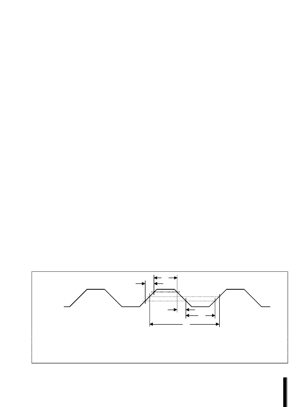
CLK
2.0V
0.8V
1.5V
T
z
T
x
T
y
T
v
T
w
Tv = t5, t49, t60e
Tw = t4, t48, t60f
Tx = t3, t47, t60d
Ty = t1, t45, t60b
Tz = t2, t46, t60c
Figure 4. Clock Waveform
相關(guān)PDF資料 |
PDF描述 |
|---|---|
| pentium processor | 32 Bit Processor With MMX And Mobile Module(32位帶移動模塊和MMX技術(shù)CPU) |
| PESD0603-140 | Raychem Overvoltage Devices |
| PESD5V2S18U | ESD protection array |
| PESDXL4UW | Low capacitance quadruple ESD protection array |
| PESDXL4UG | Low capacitance quadruple ESD protection diode array in SOT353 package |
相關(guān)代理商/技術(shù)參數(shù) |
參數(shù)描述 |
|---|---|
| P-ENV568K3G3 | 制造商:Panasonic Industrial Company 功能描述:TUNER |
| PEO14012 | 制造商:TE Connectivity 功能描述:RELAY SPCO 12VDC |
| PEO14024 | 制造商:TE Connectivity 功能描述:RELAY SPCO 24VDC |
| PEO96742 | 制造商:Delphi Corporation 功能描述:ASM TERM |
| PEOODO3A | 制造商:MACOM 制造商全稱:Tyco Electronics 功能描述:Versatile Power Entry Module with Small Footprint |
發(fā)布緊急采購,3分鐘左右您將得到回復(fù)。