- 您現(xiàn)在的位置:買賣IC網(wǎng) > PDF目錄299522 > MT47H32M16BT-37VL:A 32M X 16 DDR DRAM, 0.5 ns, PBGA92 PDF資料下載
參數(shù)資料
| 型號: | MT47H32M16BT-37VL:A |
| 元件分類: | DRAM |
| 英文描述: | 32M X 16 DDR DRAM, 0.5 ns, PBGA92 |
| 封裝: | 11 X 19 MM, LEAD FREE, FBGA-92 |
| 文件頁數(shù): | 68/126頁 |
| 文件大小: | 7045K |
第1頁第2頁第3頁第4頁第5頁第6頁第7頁第8頁第9頁第10頁第11頁第12頁第13頁第14頁第15頁第16頁第17頁第18頁第19頁第20頁第21頁第22頁第23頁第24頁第25頁第26頁第27頁第28頁第29頁第30頁第31頁第32頁第33頁第34頁第35頁第36頁第37頁第38頁第39頁第40頁第41頁第42頁第43頁第44頁第45頁第46頁第47頁第48頁第49頁第50頁第51頁第52頁第53頁第54頁第55頁第56頁第57頁第58頁第59頁第60頁第61頁第62頁第63頁第64頁第65頁第66頁第67頁當(dāng)前第68頁第69頁第70頁第71頁第72頁第73頁第74頁第75頁第76頁第77頁第78頁第79頁第80頁第81頁第82頁第83頁第84頁第85頁第86頁第87頁第88頁第89頁第90頁第91頁第92頁第93頁第94頁第95頁第96頁第97頁第98頁第99頁第100頁第101頁第102頁第103頁第104頁第105頁第106頁第107頁第108頁第109頁第110頁第111頁第112頁第113頁第114頁第115頁第116頁第117頁第118頁第119頁第120頁第121頁第122頁第123頁第124頁第125頁第126頁
pdf: 09005aef8117c18e, source: 09005aef8117c192
Micron Technology, Inc., reserves the right to change products or specifications without notice.
512MbDDR2_2.fm - Rev. H 7/05 EN
46
2004, 2005 Micron Technology, Inc. All rights reserved.
512Mb: x4, x8, x16 DDR2 SDRAM
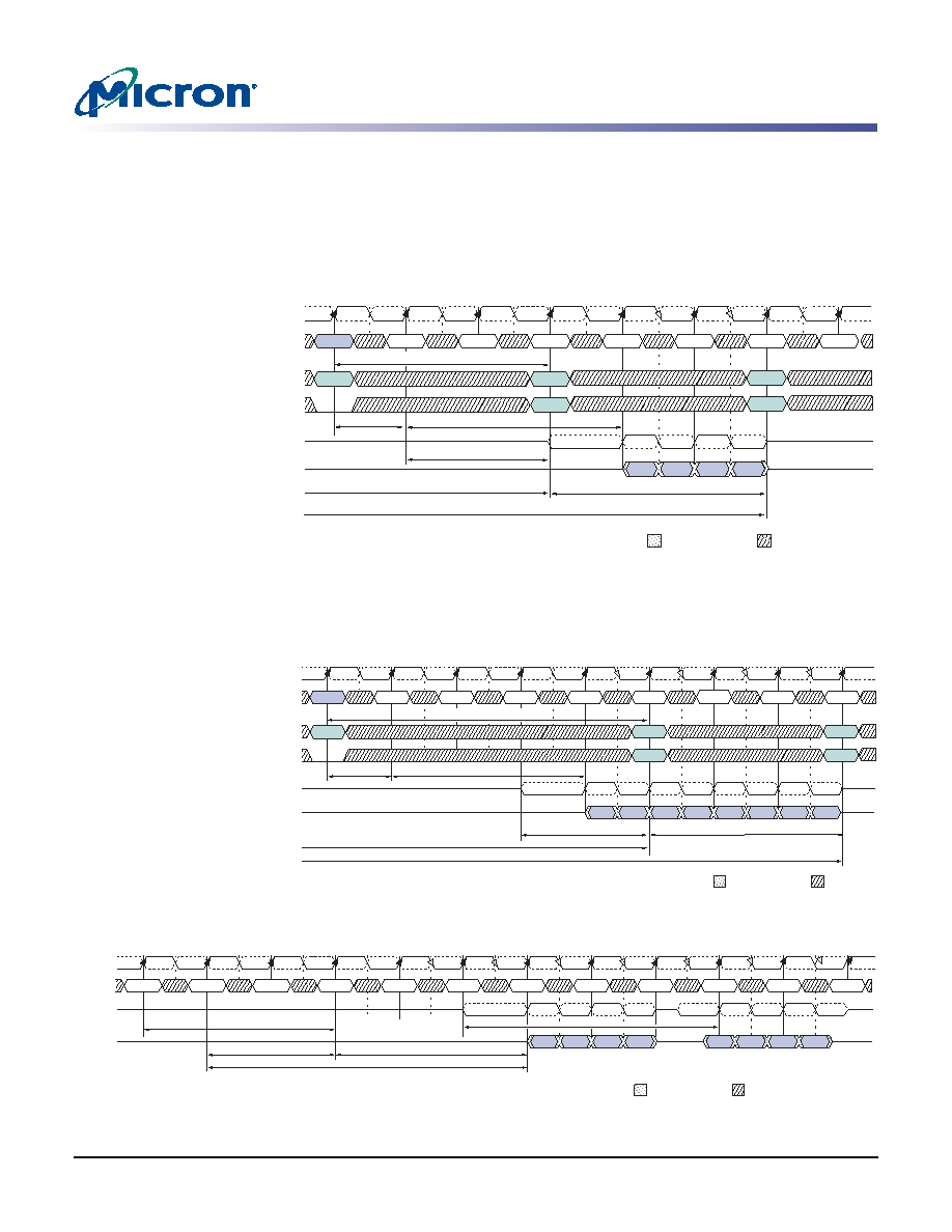
READs
tRP)* (see Figure 25 on page 46); where * means each parameter term is divided by tCK
and rounded up to the next integer. In any event, internal precharge does not start ear-
lier than two clocks after the last 4-bit prefetch.
Figure 24:
READ to PRECHARGE BL = 4
Figure 25:
READ to PRECHARGE BL = 8
Figure 26:
READ to WRITE
DOUT
CK
CK#
COMMAND
DQ
DQS, DQS#
CL = 3
READ
Read Latency = 4 (AL = 1, CL = 3), BL = 4, tRTP
≥ 2 clocks
Shown with nominal tAC, tDQSCK, and tDQSQ
T0
T1
T2
DON’T CARE
TRANSITIONING DATA
NOP
PRECHARGE
DOUT
T3
T4
T5
T6
ACTIVE
T7
ADDRESS
A10
AL = 1
NOP
Bank a
≥tRTP (MIN)
Bank a
≥tRAS (MIN)
Bank a
≥tRP (MIN)
NOP
AL + BL/2 + tRTP - 2 clocks
NOP
≥tRC (MIN)
4-bit
prefetch
Valid
DOUT
CK
CK#
COMMAND
DQ
DQS, DQS#
CL = 3
READ
RL = 4 (AL = 1, CL = 3), BL = 8, tRTP
≥ 2 clocks
Shown with nominal tAC, tDQSCK, and tDQSQ
T0
T1
T2
DON’T CARE
TRANSITIONING DATA
NOP
DOUT
T3
T4
T5
T6
T7
T8
ADDRESS
A10
AL = 1
NOP
Bank a
≥tRC (MIN)
≥tRTP (MIN)
NOP
DOUT
first 4-bit
prefetch
second 4-bit
prefetch
≥tRP (MIN)
PRECHARGE
Bank a
NOP
AL + BL/2 + tRTP - 2 clocks
NOP
ACTIVE
≥tRAS (MIN)
Valid
DOUT
n + 3
DOUT
n + 2
DOUT
n + 1
CK
CK#
COMMAND
DQ
DQS, DQS#
AL = 2
ACTIVE n
BL = 4
Shown with nominal tAC, tDQSCK, and tDQSQ
T0
T1
T2
DON’T CARE
TRANSITIONING DATA
NOP
DOUT
n
T3
T4
T5
NOP
WRITE n
T6
NOP
Din
n + 3
Din
n + 2
Din
n + 1
WL = RL - 1 = 4
T7
T8
NOP
Din
n
T9
T10
T11
NOP
CL = 3
RL = 5
CL = 3
AL = 2
tRCD = 3
READ n
相關(guān)PDF資料 |
PDF描述 |
|---|---|
| MT47H64M16HQ-3IT:G | 64M X 16 DDR DRAM, 0.4 ns, PBGA60 |
| MT47H64M8CF-5EAT:F | DDR DRAM, PBGA60 |
| MT48H16M16LFBF-10IT | 16M X 16 SYNCHRONOUS DRAM, 7 ns, PBGA54 |
| MT48LC8M16A2BB-6ALIT:G | 8M X 16 SYNCHRONOUS DRAM, 5.4 ns, PBGA60 |
| MT49H8M36HU-33 | 8M X 36 DDR DRAM, 0.3 ns, PBGA144 |
相關(guān)代理商/技術(shù)參數(shù) |
參數(shù)描述 |
|---|---|
| MT47H32M16CC-37E | 制造商:Micron Technology Inc 功能描述: |
發(fā)布緊急采購,3分鐘左右您將得到回復(fù)。