- 您現(xiàn)在的位置:買賣IC網(wǎng) > PDF目錄299522 > MT47H32M16BT-37VL:A 32M X 16 DDR DRAM, 0.5 ns, PBGA92 PDF資料下載
參數(shù)資料
| 型號: | MT47H32M16BT-37VL:A |
| 元件分類: | DRAM |
| 英文描述: | 32M X 16 DDR DRAM, 0.5 ns, PBGA92 |
| 封裝: | 11 X 19 MM, LEAD FREE, FBGA-92 |
| 文件頁數(shù): | 34/126頁 |
| 文件大小: | 7045K |
第1頁第2頁第3頁第4頁第5頁第6頁第7頁第8頁第9頁第10頁第11頁第12頁第13頁第14頁第15頁第16頁第17頁第18頁第19頁第20頁第21頁第22頁第23頁第24頁第25頁第26頁第27頁第28頁第29頁第30頁第31頁第32頁第33頁當(dāng)前第34頁第35頁第36頁第37頁第38頁第39頁第40頁第41頁第42頁第43頁第44頁第45頁第46頁第47頁第48頁第49頁第50頁第51頁第52頁第53頁第54頁第55頁第56頁第57頁第58頁第59頁第60頁第61頁第62頁第63頁第64頁第65頁第66頁第67頁第68頁第69頁第70頁第71頁第72頁第73頁第74頁第75頁第76頁第77頁第78頁第79頁第80頁第81頁第82頁第83頁第84頁第85頁第86頁第87頁第88頁第89頁第90頁第91頁第92頁第93頁第94頁第95頁第96頁第97頁第98頁第99頁第100頁第101頁第102頁第103頁第104頁第105頁第106頁第107頁第108頁第109頁第110頁第111頁第112頁第113頁第114頁第115頁第116頁第117頁第118頁第119頁第120頁第121頁第122頁第123頁第124頁第125頁第126頁
pdf: 09005aef8117c18e, source: 09005aef8117c192
Micron Technology, Inc., reserves the right to change products or specifications without notice.
512MbDDR2_2.fm - Rev. H 7/05 EN
15
2004, 2005 Micron Technology, Inc. All rights reserved.
512Mb: x4, x8, x16 DDR2 SDRAM
General Description
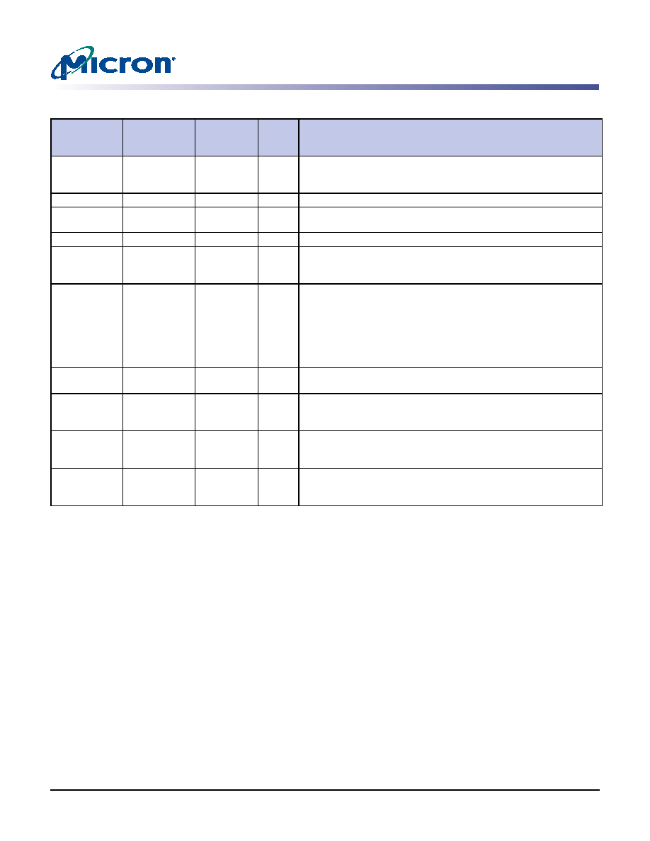
D9,F1,F3,F7,
F9,H9,K1,K3,
K7,K9
D9,H9,K1,
K3,K7,K9
VDDQ
Supply DQ Power Supply: 1.8V ±0.1V. Isolated on the device for improved
noise immunity.
M2
VREF
Supply SSTL_18 reference voltage.
D3,H3,M3,T1,
U9
D3,H3,M3,T1,
U9
VSS
Supply Ground.
M7
VSSDL
Supply DLL Ground. Isolated on the device from VSS and VSSQ.
D7,E2,E8,G2,
G8,H7, J2,J8,
L2,L8
D7,H7,J2,
J8,L2,L8
VSSQ
Supply DQ Ground. Isolated on the device for improved noise immunity.
A1,A2,A8,A9
D2,H2,V8,
AA1,AA2,AA8,
AA9
A1,A2,A8,A9,
D2,D8,E1-E3,
E7-E9,F1-F3,
F7-F9, G1-G3,
G7-G9,
AA1,AA2,AA8,
AA9
NC
–
No Connect: These pins should be left unconnected.
–
J1, J9, L1, L9,
H2,
NF
–
No Function: These pins are used as DQ4–DQ7 on the 64 Meg x 8,
but are NF (No Function) on the 128 Meg x 4 configuration.
D8, H8
–
NU
–
Not Used: Not used only on x16. If EMR[E10] = 0, D8 and H8 are
UDQS# and LDQS#.
If EMR[E10] = 1, then D8 and H8 are not used.
–
H2, H8
NU
–
Not Used: Not used only on x8. If EMR[E10] = 0, H2 and H8 are
RDQS# and DQS#.
If EMR[E10] = 1, then H2 and H8 are not used.
V3, V7, P1
RFU
–
Reserved for Future Use: row address bits A14(V3) and A15(V7) are
reserved for 2Gb and 4Gb densities. BA2 (P1) reserved for 1Gb
device.
Table 3:
FBGA 92-Ball Descriptions 128 Meg x 4, 64 Meg x 8, 32 Meg x 16
x16 FBGA
Ball
Assignment
x4, x8 FBGA
Ball
Assignment
Symbol
Type
Description
相關(guān)PDF資料 |
PDF描述 |
|---|---|
| MT47H64M16HQ-3IT:G | 64M X 16 DDR DRAM, 0.4 ns, PBGA60 |
| MT47H64M8CF-5EAT:F | DDR DRAM, PBGA60 |
| MT48H16M16LFBF-10IT | 16M X 16 SYNCHRONOUS DRAM, 7 ns, PBGA54 |
| MT48LC8M16A2BB-6ALIT:G | 8M X 16 SYNCHRONOUS DRAM, 5.4 ns, PBGA60 |
| MT49H8M36HU-33 | 8M X 36 DDR DRAM, 0.3 ns, PBGA144 |
相關(guān)代理商/技術(shù)參數(shù) |
參數(shù)描述 |
|---|---|
| MT47H32M16CC-37E | 制造商:Micron Technology Inc 功能描述: |
發(fā)布緊急采購,3分鐘左右您將得到回復(fù)。