- 您現(xiàn)在的位置:買(mǎi)賣(mài)IC網(wǎng) > PDF目錄299522 > MT47H32M16BT-37VL:A 32M X 16 DDR DRAM, 0.5 ns, PBGA92 PDF資料下載
參數(shù)資料
| 型號(hào): | MT47H32M16BT-37VL:A |
| 元件分類: | DRAM |
| 英文描述: | 32M X 16 DDR DRAM, 0.5 ns, PBGA92 |
| 封裝: | 11 X 19 MM, LEAD FREE, FBGA-92 |
| 文件頁(yè)數(shù): | 112/126頁(yè) |
| 文件大小: | 7045K |
第1頁(yè)第2頁(yè)第3頁(yè)第4頁(yè)第5頁(yè)第6頁(yè)第7頁(yè)第8頁(yè)第9頁(yè)第10頁(yè)第11頁(yè)第12頁(yè)第13頁(yè)第14頁(yè)第15頁(yè)第16頁(yè)第17頁(yè)第18頁(yè)第19頁(yè)第20頁(yè)第21頁(yè)第22頁(yè)第23頁(yè)第24頁(yè)第25頁(yè)第26頁(yè)第27頁(yè)第28頁(yè)第29頁(yè)第30頁(yè)第31頁(yè)第32頁(yè)第33頁(yè)第34頁(yè)第35頁(yè)第36頁(yè)第37頁(yè)第38頁(yè)第39頁(yè)第40頁(yè)第41頁(yè)第42頁(yè)第43頁(yè)第44頁(yè)第45頁(yè)第46頁(yè)第47頁(yè)第48頁(yè)第49頁(yè)第50頁(yè)第51頁(yè)第52頁(yè)第53頁(yè)第54頁(yè)第55頁(yè)第56頁(yè)第57頁(yè)第58頁(yè)第59頁(yè)第60頁(yè)第61頁(yè)第62頁(yè)第63頁(yè)第64頁(yè)第65頁(yè)第66頁(yè)第67頁(yè)第68頁(yè)第69頁(yè)第70頁(yè)第71頁(yè)第72頁(yè)第73頁(yè)第74頁(yè)第75頁(yè)第76頁(yè)第77頁(yè)第78頁(yè)第79頁(yè)第80頁(yè)第81頁(yè)第82頁(yè)第83頁(yè)第84頁(yè)第85頁(yè)第86頁(yè)第87頁(yè)第88頁(yè)第89頁(yè)第90頁(yè)第91頁(yè)第92頁(yè)第93頁(yè)第94頁(yè)第95頁(yè)第96頁(yè)第97頁(yè)第98頁(yè)第99頁(yè)第100頁(yè)第101頁(yè)第102頁(yè)第103頁(yè)第104頁(yè)第105頁(yè)第106頁(yè)第107頁(yè)第108頁(yè)第109頁(yè)第110頁(yè)第111頁(yè)當(dāng)前第112頁(yè)第113頁(yè)第114頁(yè)第115頁(yè)第116頁(yè)第117頁(yè)第118頁(yè)第119頁(yè)第120頁(yè)第121頁(yè)第122頁(yè)第123頁(yè)第124頁(yè)第125頁(yè)第126頁(yè)
pdf: 09005aef8117c18e, source: 09005aef8117c192
Micron Technology, Inc., reserves the right to change products or specifications without notice.
512MbDDR2_3.fm - Rev. H 7/05 EN
86
2004, 2005 Micron Technology, Inc. All rights reserved.
512Mb: x4, x8, x16 DDR2 SDRAM
Input Electrical Characteristics and Operating Conditions
Notes: 1. VIN(DC) specifies the allowable DC execution of each input of differential pair such as CK,
CK#, DQS, DQS#, LDQS, LDQS#, UDQS, UDQS#, and RDQS, RDQS#.
2. VID(DC) specifies the input differential voltage | VTR - VCP | required for switching, where
VTR is the true input (such as CK, DQS, LDQS, UDQS) level and VCP is the complementary
input (such as CK#, DQS#, LDQS#, UDQS#). The minimum value is equal to VIH(DC) - VIL(DC).
Differential input signal levels are shown in Figure 67.
3. VID(AC) specifies the input differential voltage | VTR - VCP | required for switching, where
VTR is the true input (such as CK, DQS, LDQS, UDQS, RDQS) level and VCP is the complemen-
tary input (such as CK#, DQS#, LDQS#, UDQS#, RDQS#). The minimum value is equal to
VIH(AC) - VIL(AC), as shown in Table 21 on page 85.
4. The typical value of VIX(AC) is expected to be about 0.5 x VDDQ of the transmitting device
and VIX(AC) is expected to track variations in VDDQ. VIX(AC) indicates the voltage at which
differential input signals must cross, as shown in Figure 67.
5. VMP(DC) specifies the input differential common mode voltage (VTR + VCP)/2 where VTR is
the true input (CK, DQS) level and VCP is the complementary input (CK#, DQS#). VMP(DC) is
expected to be approximately 0.5 x VDDQ.
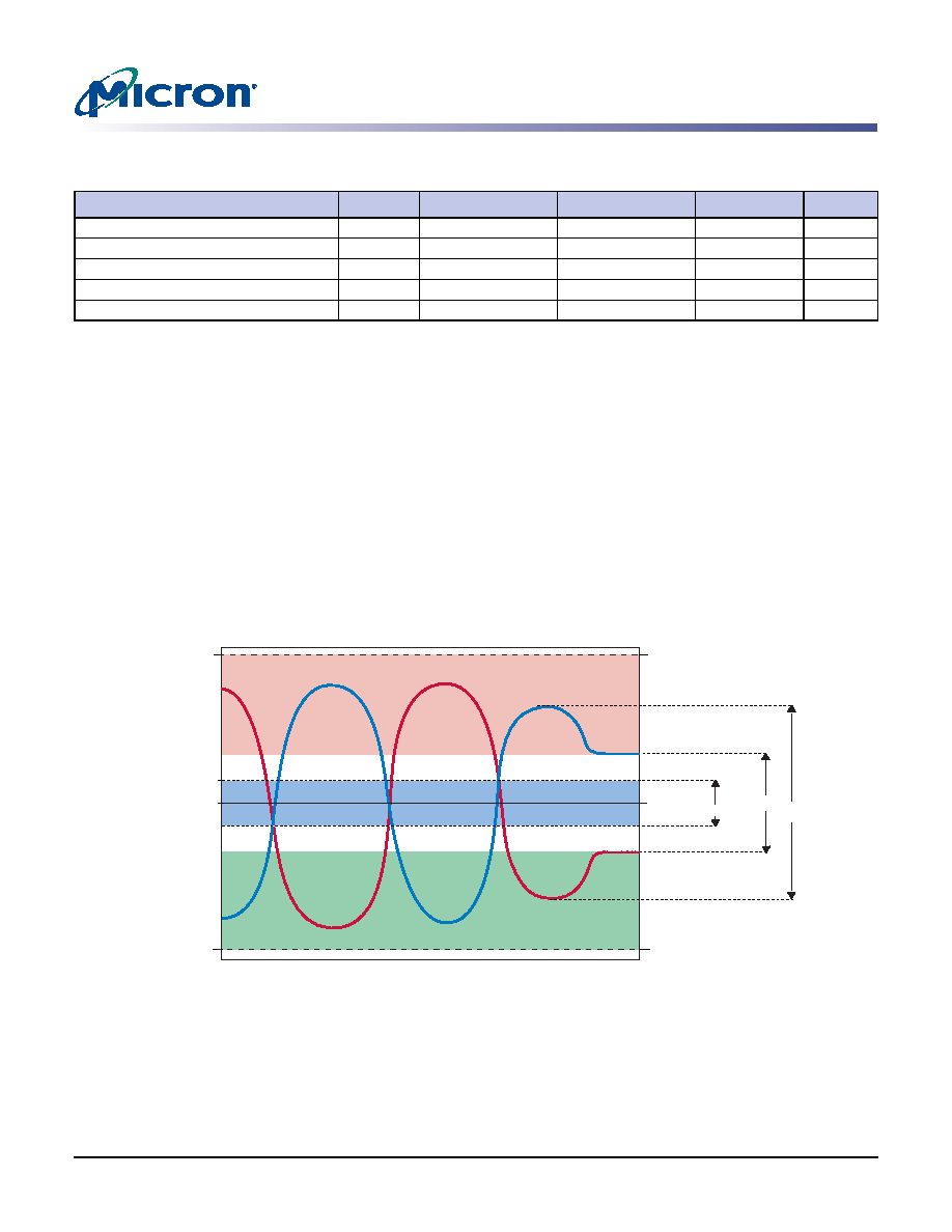
Figure 67:
Differential Input Signal Levels
Notes: 1. This provides a minimum of 850mV to a maximum of 950mV and is expected to be VDDQ/2.
2. TR and CP must cross in this region.
3. TR and CP must meet at least VID(DC) MIN when static and is centered around VMP(DC).
4. TR and CP must have a minimum 500mV peak-to-peak swing.
5. TR and CP may not be more positive than VDDQ + 0.3V or more negative than VSS - 0.3V.
6. For AC operation, all DC clock requirements must also be satisfied.
7. Numbers in diagram reflect nominal values.
8. TR represents the CK, DQS, RDQS, LDQS, and UDQS signals; CP represents CK#, DQS#,
RDQS#, LDQS#, and UDQS# signals.
Table 22:
Differential Input Logic Levels
All voltages referenced to VSS
Parameter
Symbol
Min
Max
Units
Notes
DC Input Signal Voltage
VIN(DC)
-300
VDDQ + 300
mV
1
DC Differential Input Voltage
VID(DC)
250
VDDQ + 600
mV
2
AC Differential Input Voltage
VID(AC)
500
VDDQ + 600
mV
3
AC Differential Cross-Point Voltage
VIX(AC)
0.50 x VDDQ - 175
0.50 x VDDQ + 175
mV
4
Input Midpoint Voltage
VMP(DC)
850
950
mV
5
CP8
TR8
2.1V
@ VDDQ = 1.8V
2
3
VIN(DC) MAX5
VIN(DC) MIN
5
4
- 0.30V
0.9V
1.075V
0.725 V
VID(AC)
VID(DC)
X
VMP(DC)1
VIX(AC)
X
相關(guān)PDF資料 |
PDF描述 |
|---|---|
| MT47H64M16HQ-3IT:G | 64M X 16 DDR DRAM, 0.4 ns, PBGA60 |
| MT47H64M8CF-5EAT:F | DDR DRAM, PBGA60 |
| MT48H16M16LFBF-10IT | 16M X 16 SYNCHRONOUS DRAM, 7 ns, PBGA54 |
| MT48LC8M16A2BB-6ALIT:G | 8M X 16 SYNCHRONOUS DRAM, 5.4 ns, PBGA60 |
| MT49H8M36HU-33 | 8M X 36 DDR DRAM, 0.3 ns, PBGA144 |
相關(guān)代理商/技術(shù)參數(shù) |
參數(shù)描述 |
|---|---|
| MT47H32M16CC-37E | 制造商:Micron Technology Inc 功能描述: |
發(fā)布緊急采購(gòu),3分鐘左右您將得到回復(fù)。