- 您現(xiàn)在的位置:買賣IC網(wǎng) > PDF目錄296642 > MT46V128M4FN-75E:C 128M X 4 DDR DRAM, 0.75 ns, PBGA60 PDF資料下載
參數(shù)資料
| 型號(hào): | MT46V128M4FN-75E:C |
| 元件分類: | DRAM |
| 英文描述: | 128M X 4 DDR DRAM, 0.75 ns, PBGA60 |
| 封裝: | 10 X 12.50 MM, FBGA-60 |
| 文件頁(yè)數(shù): | 10/94頁(yè) |
| 文件大小: | 4179K |
第1頁(yè)第2頁(yè)第3頁(yè)第4頁(yè)第5頁(yè)第6頁(yè)第7頁(yè)第8頁(yè)第9頁(yè)當(dāng)前第10頁(yè)第11頁(yè)第12頁(yè)第13頁(yè)第14頁(yè)第15頁(yè)第16頁(yè)第17頁(yè)第18頁(yè)第19頁(yè)第20頁(yè)第21頁(yè)第22頁(yè)第23頁(yè)第24頁(yè)第25頁(yè)第26頁(yè)第27頁(yè)第28頁(yè)第29頁(yè)第30頁(yè)第31頁(yè)第32頁(yè)第33頁(yè)第34頁(yè)第35頁(yè)第36頁(yè)第37頁(yè)第38頁(yè)第39頁(yè)第40頁(yè)第41頁(yè)第42頁(yè)第43頁(yè)第44頁(yè)第45頁(yè)第46頁(yè)第47頁(yè)第48頁(yè)第49頁(yè)第50頁(yè)第51頁(yè)第52頁(yè)第53頁(yè)第54頁(yè)第55頁(yè)第56頁(yè)第57頁(yè)第58頁(yè)第59頁(yè)第60頁(yè)第61頁(yè)第62頁(yè)第63頁(yè)第64頁(yè)第65頁(yè)第66頁(yè)第67頁(yè)第68頁(yè)第69頁(yè)第70頁(yè)第71頁(yè)第72頁(yè)第73頁(yè)第74頁(yè)第75頁(yè)第76頁(yè)第77頁(yè)第78頁(yè)第79頁(yè)第80頁(yè)第81頁(yè)第82頁(yè)第83頁(yè)第84頁(yè)第85頁(yè)第86頁(yè)第87頁(yè)第88頁(yè)第89頁(yè)第90頁(yè)第91頁(yè)第92頁(yè)第93頁(yè)第94頁(yè)
09005aef80a1d9e7
Micron Technology, Inc., reserves the right to change products or specifications without notice.
512MBDDRx4x8x16_2.fm - Rev. J 1/06 EN
18
2000–2005 Micron Technology, Inc. All rights reserved.
512Mb: x4, x8, x16 DDR SDRAM
Register Definition
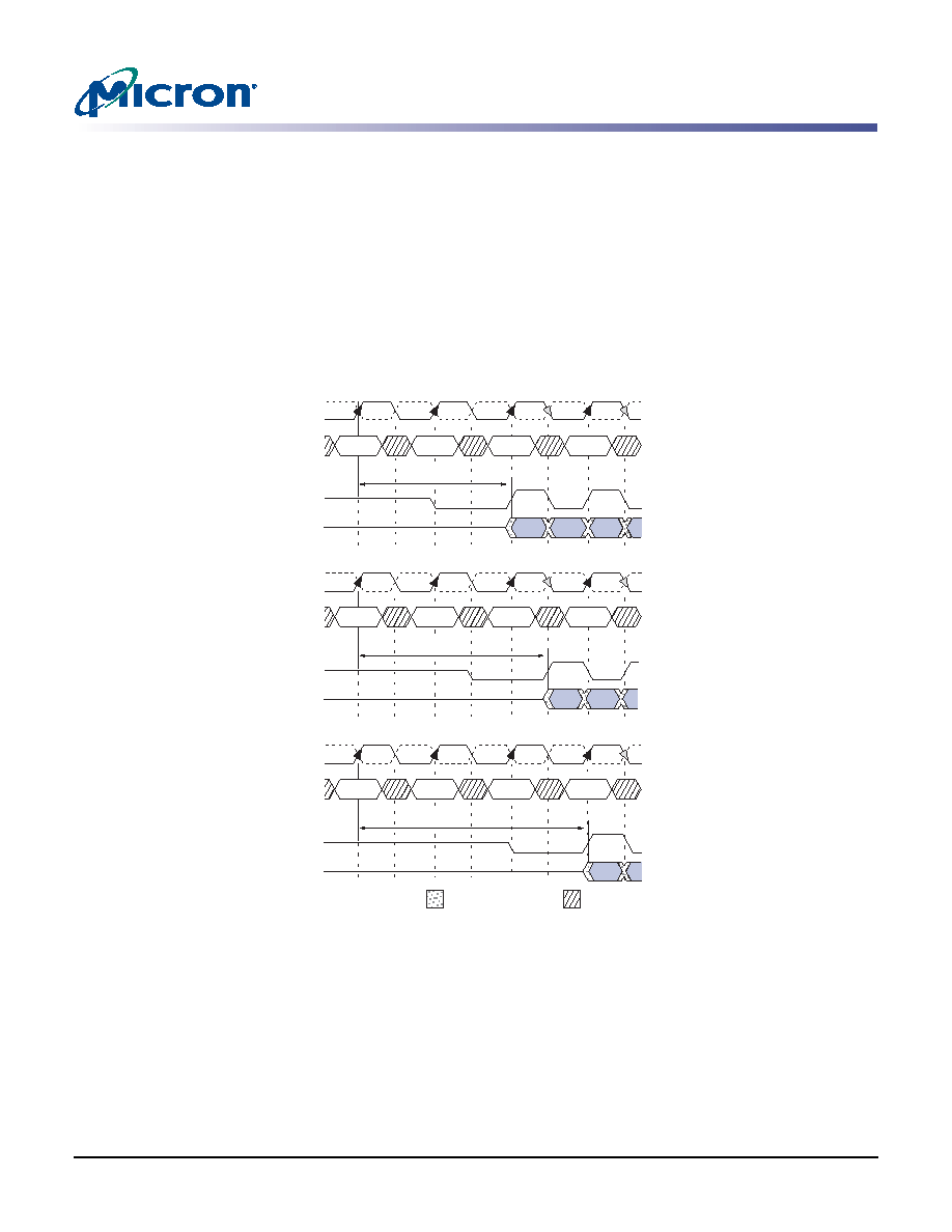
CAS (READ) Latency
The READ latency is the delay, in clock cycles, between the registration of a READ com-
mand and the availability of the first bit of output data. The latency can be set to 2, 2.5, or
3 (DDR400 only) clocks, as shown in Figure 8.
If a READ command is registered at clock edge n, and the latency is m clocks, the data
will be available nominally coincident with clock edge n + m. Table 5 on page 19 indi-
cates the operating frequencies at which each CAS latency (CL) setting can be used.
Reserved states should not be used, as unknown operation or incompatibility with
future versions may result.
Figure 8:
CAS Latency (CL)
Note:
Burst Length = 4 in the cases shown; shown with nominal tAC, tDQSCK, and tDQSQ.
CK
CK#
COMMAND
DQ
DQS
CL = 2
READ
NOP
READ
NOP
CK
CK#
COMMAND
DQ
DQS
CL = 2.5
T0
T1
T2
T2n
T3
T3n
T0
T1
T2
T2n
T3
T3n
DON’T CARE
TRANSITIONING DATA
READ
NOP
CK
CK#
COMMAND
DQ
DQS
CL = 3
T0
T1
T2
T3
T3n
相關(guān)PDF資料 |
PDF描述 |
|---|---|
| MT46V128M4P-75L:C | 128M X 4 DDR DRAM, 0.75 ns, PDSO66 |
| MT46V128M4P-75ZLIT:C | 128M X 4 DDR DRAM, 0.75 ns, PDSO66 |
| MT46V64M4TG-75E | 64M X 4 DDR DRAM, 0.75 ns, PDSO66 |
| MT46V64M4FG-75Z | 64M X 4 DDR DRAM, 0.75 ns, PBGA60 |
| MT47H128M8HQ-3AT | 128M X 8 DDR DRAM, 0.4 ns, PBGA60 |
相關(guān)代理商/技術(shù)參數(shù) |
參數(shù)描述 |
|---|
發(fā)布緊急采購(gòu),3分鐘左右您將得到回復(fù)。