- 您現(xiàn)在的位置:買賣IC網(wǎng) > PDF目錄69020 > MB89PV980-201 8-BIT, 4.2 MHz, MICROCONTROLLER, CQFP64 PDF資料下載
參數(shù)資料
| 型號(hào): | MB89PV980-201 |
| 元件分類: | 微控制器/微處理器 |
| 英文描述: | 8-BIT, 4.2 MHz, MICROCONTROLLER, CQFP64 |
| 封裝: | 1 MM PITCH, CERAMIC, PIGGY BACK, MQFP-64 |
| 文件頁數(shù): | 141/426頁 |
| 文件大?。?/td> | 2051K |
| 代理商: | MB89PV980-201 |
第1頁第2頁第3頁第4頁第5頁第6頁第7頁第8頁第9頁第10頁第11頁第12頁第13頁第14頁第15頁第16頁第17頁第18頁第19頁第20頁第21頁第22頁第23頁第24頁第25頁第26頁第27頁第28頁第29頁第30頁第31頁第32頁第33頁第34頁第35頁第36頁第37頁第38頁第39頁第40頁第41頁第42頁第43頁第44頁第45頁第46頁第47頁第48頁第49頁第50頁第51頁第52頁第53頁第54頁第55頁第56頁第57頁第58頁第59頁第60頁第61頁第62頁第63頁第64頁第65頁第66頁第67頁第68頁第69頁第70頁第71頁第72頁第73頁第74頁第75頁第76頁第77頁第78頁第79頁第80頁第81頁第82頁第83頁第84頁第85頁第86頁第87頁第88頁第89頁第90頁第91頁第92頁第93頁第94頁第95頁第96頁第97頁第98頁第99頁第100頁第101頁第102頁第103頁第104頁第105頁第106頁第107頁第108頁第109頁第110頁第111頁第112頁第113頁第114頁第115頁第116頁第117頁第118頁第119頁第120頁第121頁第122頁第123頁第124頁第125頁第126頁第127頁第128頁第129頁第130頁第131頁第132頁第133頁第134頁第135頁第136頁第137頁第138頁第139頁第140頁當(dāng)前第141頁第142頁第143頁第144頁第145頁第146頁第147頁第148頁第149頁第150頁第151頁第152頁第153頁第154頁第155頁第156頁第157頁第158頁第159頁第160頁第161頁第162頁第163頁第164頁第165頁第166頁第167頁第168頁第169頁第170頁第171頁第172頁第173頁第174頁第175頁第176頁第177頁第178頁第179頁第180頁第181頁第182頁第183頁第184頁第185頁第186頁第187頁第188頁第189頁第190頁第191頁第192頁第193頁第194頁第195頁第196頁第197頁第198頁第199頁第200頁第201頁第202頁第203頁第204頁第205頁第206頁第207頁第208頁第209頁第210頁第211頁第212頁第213頁第214頁第215頁第216頁第217頁第218頁第219頁第220頁第221頁第222頁第223頁第224頁第225頁第226頁第227頁第228頁第229頁第230頁第231頁第232頁第233頁第234頁第235頁第236頁第237頁第238頁第239頁第240頁第241頁第242頁第243頁第244頁第245頁第246頁第247頁第248頁第249頁第250頁第251頁第252頁第253頁第254頁第255頁第256頁第257頁第258頁第259頁第260頁第261頁第262頁第263頁第264頁第265頁第266頁第267頁第268頁第269頁第270頁第271頁第272頁第273頁第274頁第275頁第276頁第277頁第278頁第279頁第280頁第281頁第282頁第283頁第284頁第285頁第286頁第287頁第288頁第289頁第290頁第291頁第292頁第293頁第294頁第295頁第296頁第297頁第298頁第299頁第300頁第301頁第302頁第303頁第304頁第305頁第306頁第307頁第308頁第309頁第310頁第311頁第312頁第313頁第314頁第315頁第316頁第317頁第318頁第319頁第320頁第321頁第322頁第323頁第324頁第325頁第326頁第327頁第328頁第329頁第330頁第331頁第332頁第333頁第334頁第335頁第336頁第337頁第338頁第339頁第340頁第341頁第342頁第343頁第344頁第345頁第346頁第347頁第348頁第349頁第350頁第351頁第352頁第353頁第354頁第355頁第356頁第357頁第358頁第359頁第360頁第361頁第362頁第363頁第364頁第365頁第366頁第367頁第368頁第369頁第370頁第371頁第372頁第373頁第374頁第375頁第376頁第377頁第378頁第379頁第380頁第381頁第382頁第383頁第384頁第385頁第386頁第387頁第388頁第389頁第390頁第391頁第392頁第393頁第394頁第395頁第396頁第397頁第398頁第399頁第400頁第401頁第402頁第403頁第404頁第405頁第406頁第407頁第408頁第409頁第410頁第411頁第412頁第413頁第414頁第415頁第416頁第417頁第418頁第419頁第420頁第421頁第422頁第423頁第424頁第425頁第426頁
221
8.3 Structure of 8/16-bit Timer/Counter
8.3
Structure of 8/16-bit Timer/Counter
This section describes the pins, pin block diagram, registers, and interrupt source of
the 8/16-bit Timer/Counter.
s 8/16-bit Timer/Counter Pins
The 8/16-bit timer/counter uses the P20/EC and P22/TO pins. The P20/EC pin can function
either as a general-purpose I/O port (P20), as the external clock input pin of timer (EC). The
P22/TO pin can function either as general-purpose I/O port (P22), as the square wave output
pin of time (TO).
EC:
In the 8-bit timer 1 or 16-bit mode, if external clock input (counter function) is selected (T1CR:
T1CS1 = 11B, T1CS0 = 11B), the counter counts the external clocks applied to this pin. The
P20/EC pin sets the pin as an input port in the port data direction register DDR2: bit 0 = "0"
when using as the EC pin.
TO:
In the 8-bit timer 1 or 16-bit mode, a square wave is output at this pin. Enabling square wave
output (T1CR: T1OS1, T1OS0 = expect 00B) automatically sets the P22/TO pin as an output
pin, regardless of the port data direction register (DDR2: bit 2) value, and sets the pin to function
as the TO pin.
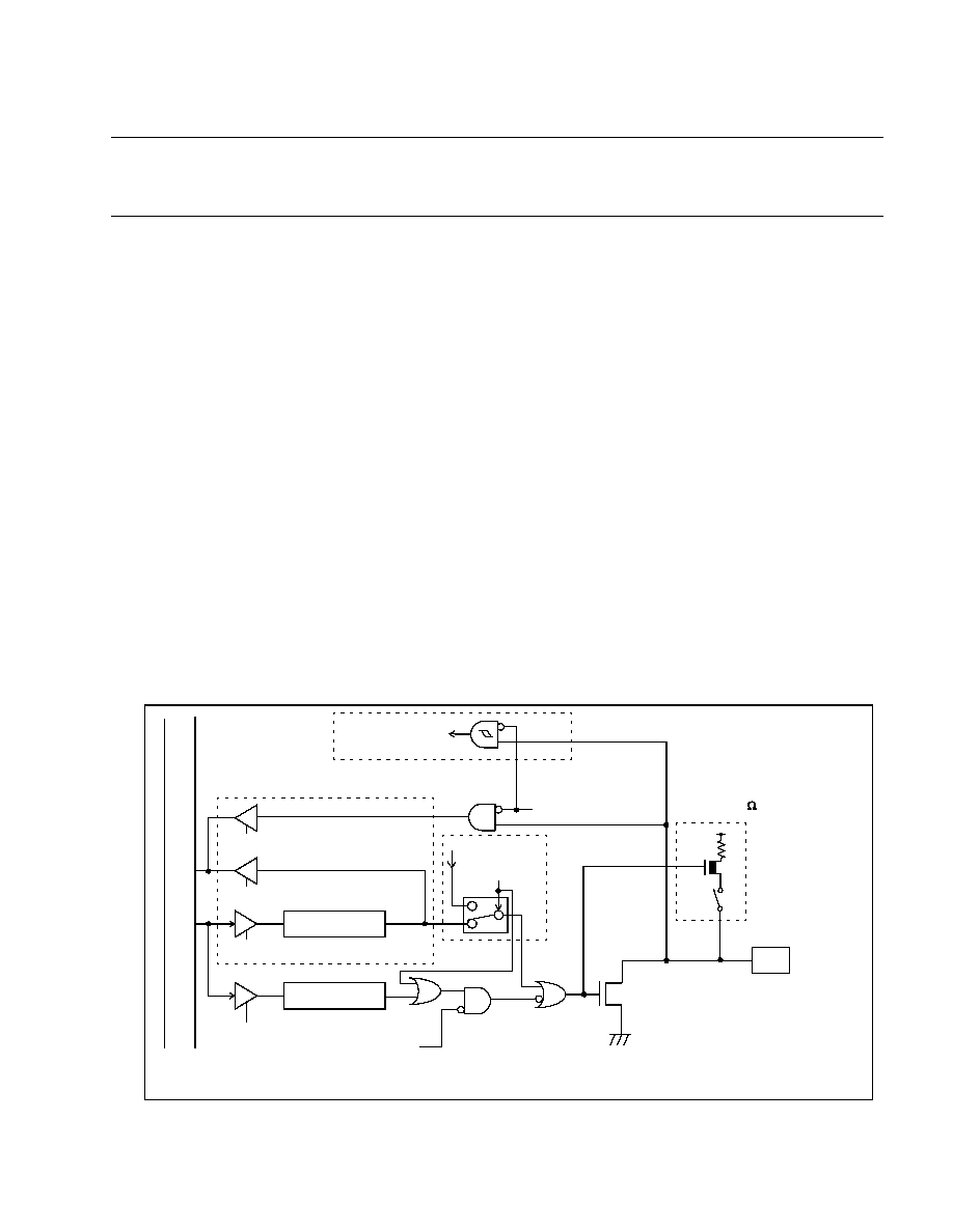
s Block Diagram of 8/16-bit Timer Counter Pins
Figure 8.3-1 Block Diagram of 8/16-Bit Timer/Counter Pins for MB89983
PDR (Port data register)
DDR
In
te
rnal
dat
a
b
u
s
PDR read
PDR read (for bit manipulation instructions)
Output latch
PDR write
DDR write
Pin
SPL: Pin state specification bit in the standby control register (STBC)
N-ch
Stop, watch mode (SPL = 1)
To peripheral input
EC pin only
(Port data direction register)
TO pin only
Stop, watch mode
Pull-up resistor
(Approx. 50 k
/5.0 V)
R
P20/EC
P22/TO
Timer output
output enable
signal
相關(guān)PDF資料 |
PDF描述 |
|---|---|
| MB89P985PFV-101 | 8-BIT, OTPROM, 4.2 MHz, MICROCONTROLLER, PQFP64 |
| MB89983-XXX-PFM | 8-BIT, MROM, 4.2 MHz, MICROCONTROLLER, PQFP64 |
| MB89P985PFM-201 | 8-BIT, OTPROM, 4.2 MHz, MICROCONTROLLER, PQFP64 |
| MB89PV930ACF | 8-BIT, 10 MHz, MICROCONTROLLER, CQFP48 |
| MB89T627RP-SH | 8-BIT, 10 MHz, MICROCONTROLLER, PDIP64 |
相關(guān)代理商/技術(shù)參數(shù) |
參數(shù)描述 |
|---|---|
| MB89PW625 | 制造商:FUJITSU 制造商全稱:Fujitsu Component Limited. 功能描述:8-bit Proprietary Microcontroller |
| MB89R112B1QN-G-AMERE1 | 制造商:FUJITSU 功能描述: |
| MB89R112B2QN-G-AMERE1 | 制造商:FUJITSU 功能描述: |
| MB89T637R-101P-G-SH | 制造商:FUJITSU 功能描述: |
| MB89T637R-102P-G-SH-E1 | 制造商:FUJITSU 功能描述: |
發(fā)布緊急采購(gòu),3分鐘左右您將得到回復(fù)。