- 您現(xiàn)在的位置:買賣IC網(wǎng) > PDF目錄296260 > K4J52324KI-HC1A0 512M X 1 DDR DRAM, 0.2 ns, PBGA136 PDF資料下載
參數(shù)資料
| 型號: | K4J52324KI-HC1A0 |
| 元件分類: | DRAM |
| 英文描述: | 512M X 1 DDR DRAM, 0.2 ns, PBGA136 |
| 封裝: | HALOGEN FREE AND ROHS COMPLIANT, FBGA-136 |
| 文件頁數(shù): | 22/61頁 |
| 文件大?。?/td> | 1364K |
| 代理商: | K4J52324KI-HC1A0 |
第1頁第2頁第3頁第4頁第5頁第6頁第7頁第8頁第9頁第10頁第11頁第12頁第13頁第14頁第15頁第16頁第17頁第18頁第19頁第20頁第21頁當(dāng)前第22頁第23頁第24頁第25頁第26頁第27頁第28頁第29頁第30頁第31頁第32頁第33頁第34頁第35頁第36頁第37頁第38頁第39頁第40頁第41頁第42頁第43頁第44頁第45頁第46頁第47頁第48頁第49頁第50頁第51頁第52頁第53頁第54頁第55頁第56頁第57頁第58頁第59頁第60頁第61頁
- 29 -
K4J52324KI
datasheet
GDDR3 SGRAM
Rev. 1.2
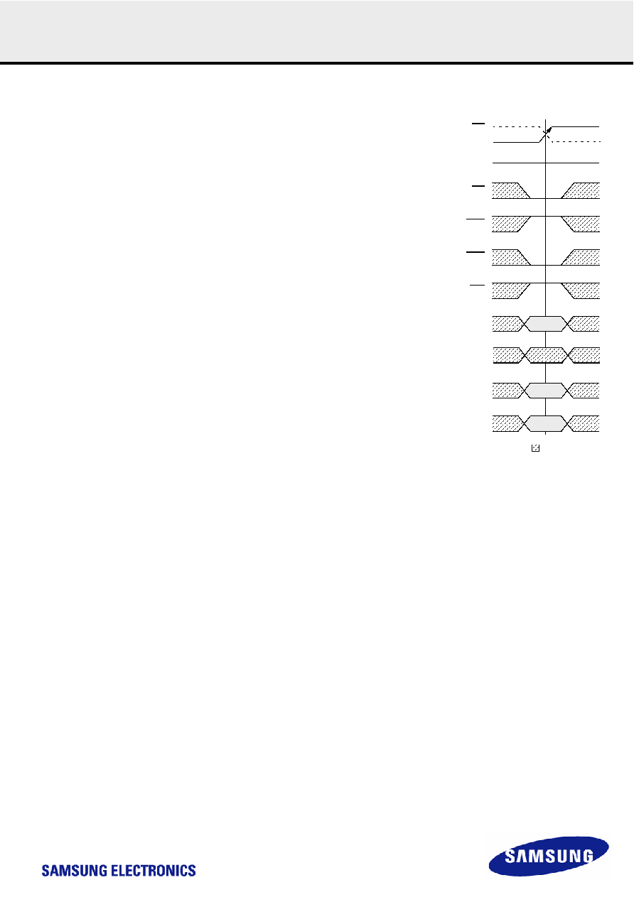
7.9.2 READs
READ bursts are initiated with a READ command, as below figure. The starting column and bank addresses
are provided with the READ command and auto precharge is either enabled or disabled for that burst access.
If auto precharge is enabled, the row being accessed is precharged at the completion of the burst after
tRAS(min) has been met. For the generic READ commands used in the following illustrations, auto precharge
is disabled.
During READ bursts, the valid data-out element from the starting column address will be available following
the CAS Latency after the READ command. Each subsequent data-out element will be valid nominally at the
next positive or negative strobe edge. READ burst figure shows general timing for 2 of the possible CAS
latency settings. The GDDR3(x32) drives the output data edge aligned to the crossing of CK and /CK and to
RDQS. The initial HIGH transition LOW of RDQS is known as the read preamble; the half cycle coincident
with the last data-out element is known as the read postamble.
Upon completion of a burst, assuming no other commands have been initiated, the DQs will go High-Z. A
detailed explanation of tDQSQ (valid data-out skew), tDV (data-out window hold), the valid data window are
depicted in Data Output Timing (1) figure. A detailed explanation of tAC (DQS and DQ transition skew to CK)
is shown in Data Output Timing (2) figure.
Data from any READ burst may be concatenated with data from a subsequent READ command. A continu-
ous flow of data can be maintained. The first data element from the new burst follows the last element of a
completed burst. The new READ command should be issued x cycles after the first READ command, where
x equals the number of data element nibbles (nibbles are required by the 4n-prefetch architecture) depending
on the burst length. This is shown in consecutive READ bursts figure. Nonconsecutive read data is shown for
illustration in nonconsecutive READ bursts figure. Full-speed random read accesses within a page (or pages)
can be performed as shown in Random READ accesses figure. Data from a READ burst cannot be termi-
nated or truncated.
During READ commands the GDDR3 DRAM disables its data terminators.
CK
CA
EN AP
DIS AP
BA
CS
RAS
CAS
WE
A0-A7, A9
A10, A11
A8
BA0,1,2
CA = Column Address
BA = Bank Address
EN AP = Enable Auto Precharge
DIS AP = Disable Auto Precharge
CKE
HIGH
READ Command
DON’T CARE
相關(guān)PDF資料 |
PDF描述 |
|---|---|
| K4M64163PK-BE900 | 4M X 16 SYNCHRONOUS DRAM, 7 ns, PBGA54 |
| K507 | 2 ELEMENT, 2000 uH, GENERAL PURPOSE INDUCTOR |
| K001 | 2 ELEMENT, 2000 uH, GENERAL PURPOSE INDUCTOR |
| K004 | 2 ELEMENT, 500 uH, GENERAL PURPOSE INDUCTOR |
| K5A22NAU | KEYPAD SWITCH, SPST, MOMENTARY, 0.1A, 50VDC, 2 N, SURFACE MOUNT-STRAIGHT |
相關(guān)代理商/技術(shù)參數(shù) |
參數(shù)描述 |
|---|---|
| K4J52324QC | 制造商:SAMSUNG 制造商全稱:Samsung semiconductor 功能描述:512Mbit GDDR3 SDRAM |
| K4J52324QC-AC20000 | 制造商:Samsung Semiconductor 功能描述:GDDR3 SDRAM X32 BOC - Trays |
| K4J52324QC-BC14 | 制造商:SAMSUNG 制造商全稱:Samsung semiconductor 功能描述:512Mbit GDDR3 SDRAM |
| K4J52324QC-BC14000 | 制造商:Samsung Semiconductor 功能描述:GDDR3 SDRAM X32 BOC LEAD PART 10W - Trays |
| K4J52324QC-BC16 | 制造商:SAMSUNG 制造商全稱:Samsung semiconductor 功能描述:512Mbit GDDR3 SDRAM |
發(fā)布緊急采購,3分鐘左右您將得到回復(fù)。