- 您現(xiàn)在的位置:買賣IC網(wǎng) > PDF目錄296260 > K4J52324KI-HC1A0 512M X 1 DDR DRAM, 0.2 ns, PBGA136 PDF資料下載
參數(shù)資料
| 型號(hào): | K4J52324KI-HC1A0 |
| 元件分類: | DRAM |
| 英文描述: | 512M X 1 DDR DRAM, 0.2 ns, PBGA136 |
| 封裝: | HALOGEN FREE AND ROHS COMPLIANT, FBGA-136 |
| 文件頁數(shù): | 21/61頁 |
| 文件大小: | 1364K |
| 代理商: | K4J52324KI-HC1A0 |
第1頁第2頁第3頁第4頁第5頁第6頁第7頁第8頁第9頁第10頁第11頁第12頁第13頁第14頁第15頁第16頁第17頁第18頁第19頁第20頁當(dāng)前第21頁第22頁第23頁第24頁第25頁第26頁第27頁第28頁第29頁第30頁第31頁第32頁第33頁第34頁第35頁第36頁第37頁第38頁第39頁第40頁第41頁第42頁第43頁第44頁第45頁第46頁第47頁第48頁第49頁第50頁第51頁第52頁第53頁第54頁第55頁第56頁第57頁第58頁第59頁第60頁第61頁
- 28 -
K4J52324KI
datasheet
GDDR3 SGRAM
Rev. 1.2
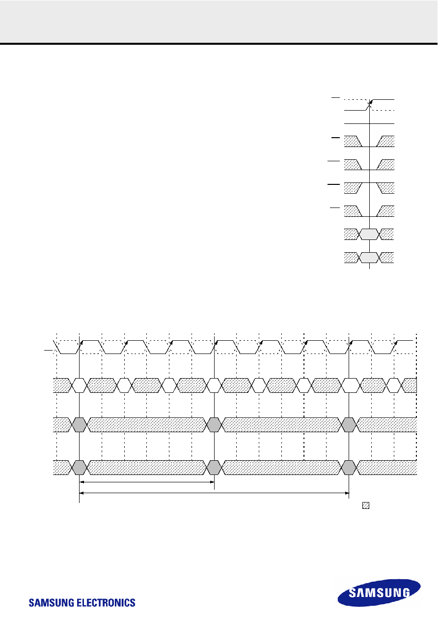
7.9 Operations
7.9.1 Bank/Row Activation
Figure 8. Example : Meeting tRCD
Before any READ or WRITE commands can be issued to a banks within the GDDR3 SGRAM, a row in that
bank must be "opened." This is accomplished via the ACTIVE command, which selects both the bank and
the row to be activated.
After a row is opened with an ACTIVE command, a READ or WRITE command may be issued to that row,
subject to the tRCD specification. tRCD(min) should be divided by the clock period and rounded up to the next
whole number to determine the earliest clock edge after the ACTIVE command in which a READ or WRITE
command can be entered. For example, a tRCD specification of 14ns with a 700MHz clock (1.4ns period)
results in 10 clocks. This is reflected in below figure, which covers any case where 10<tRCD(min)/tCK≤ 11.
The same procedure is used to convert other specification limits from time units to clock cycles).
A subsequent ACTIVE command to a different row in the same bank can only be issued after the previous
active row has been “closed”(precharged). The minimum time interval between successive ACTIVE com-
mands to the same bank is defined by tRC.
A subsequent ACTIVE command to another bank can be issued while the first bank is being accessed,
which results in a reduction of total row access overhead. The minimum time interval between successive
ACTIVE commands to different banks is defined by tRRD.
* Any system or application incorporating random access memory products should be properly designed,
tested and qualified to ensure proper use or access of such memory products. Disproportionate, excessive
and/or repeated access to a particular address or addresses may result in reduction of product life.
CK
RA
CKE
CS
RAS
CAS
WE
A0-A11
BA0,1,2
HIGH
BA
RA = Row Address
BA = Bank Address
Activating a Specific Row
in a Specific Bank
T0
T1
T3
T4
T12
CK
COMMAND
T13
A0-A11
T2
T14
ACT
NOP
ACT
NOP
RD/WR
NOP
Row
Col
BA0~BA2
Bank x
Bank y
tRRD
tRCD
DON’T CARE
CK
相關(guān)PDF資料 |
PDF描述 |
|---|---|
| K4M64163PK-BE900 | 4M X 16 SYNCHRONOUS DRAM, 7 ns, PBGA54 |
| K507 | 2 ELEMENT, 2000 uH, GENERAL PURPOSE INDUCTOR |
| K001 | 2 ELEMENT, 2000 uH, GENERAL PURPOSE INDUCTOR |
| K004 | 2 ELEMENT, 500 uH, GENERAL PURPOSE INDUCTOR |
| K5A22NAU | KEYPAD SWITCH, SPST, MOMENTARY, 0.1A, 50VDC, 2 N, SURFACE MOUNT-STRAIGHT |
相關(guān)代理商/技術(shù)參數(shù) |
參數(shù)描述 |
|---|---|
| K4J52324QC | 制造商:SAMSUNG 制造商全稱:Samsung semiconductor 功能描述:512Mbit GDDR3 SDRAM |
| K4J52324QC-AC20000 | 制造商:Samsung Semiconductor 功能描述:GDDR3 SDRAM X32 BOC - Trays |
| K4J52324QC-BC14 | 制造商:SAMSUNG 制造商全稱:Samsung semiconductor 功能描述:512Mbit GDDR3 SDRAM |
| K4J52324QC-BC14000 | 制造商:Samsung Semiconductor 功能描述:GDDR3 SDRAM X32 BOC LEAD PART 10W - Trays |
| K4J52324QC-BC16 | 制造商:SAMSUNG 制造商全稱:Samsung semiconductor 功能描述:512Mbit GDDR3 SDRAM |
發(fā)布緊急采購,3分鐘左右您將得到回復(fù)。