- 您現(xiàn)在的位置:買賣IC網(wǎng) > PDF目錄378513 > CY7C924DX (Cypress Semiconductor Corp.) 200-MBaud HOTLink Transceiver(200H波特?zé)峤硬迨瞻l(fā)器) PDF資料下載
參數(shù)資料
| 型號: | CY7C924DX |
| 廠商: | Cypress Semiconductor Corp. |
| 英文描述: | 200-MBaud HOTLink Transceiver(200H波特?zé)峤硬迨瞻l(fā)器) |
| 中文描述: | 200 MBd的的HOTLink收發(fā)器(200小時波特?zé)峤硬迨瞻l(fā)器) |
| 文件頁數(shù): | 10/58頁 |
| 文件大?。?/td> | 636K |
| 代理商: | CY7C924DX |
第1頁第2頁第3頁第4頁第5頁第6頁第7頁第8頁第9頁當(dāng)前第10頁第11頁第12頁第13頁第14頁第15頁第16頁第17頁第18頁第19頁第20頁第21頁第22頁第23頁第24頁第25頁第26頁第27頁第28頁第29頁第30頁第31頁第32頁第33頁第34頁第35頁第36頁第37頁第38頁第39頁第40頁第41頁第42頁第43頁第44頁第45頁第46頁第47頁第48頁第49頁第50頁第51頁第52頁第53頁第54頁第55頁第56頁第57頁第58頁
CY7C924DX
PRELIMINARY
10
50
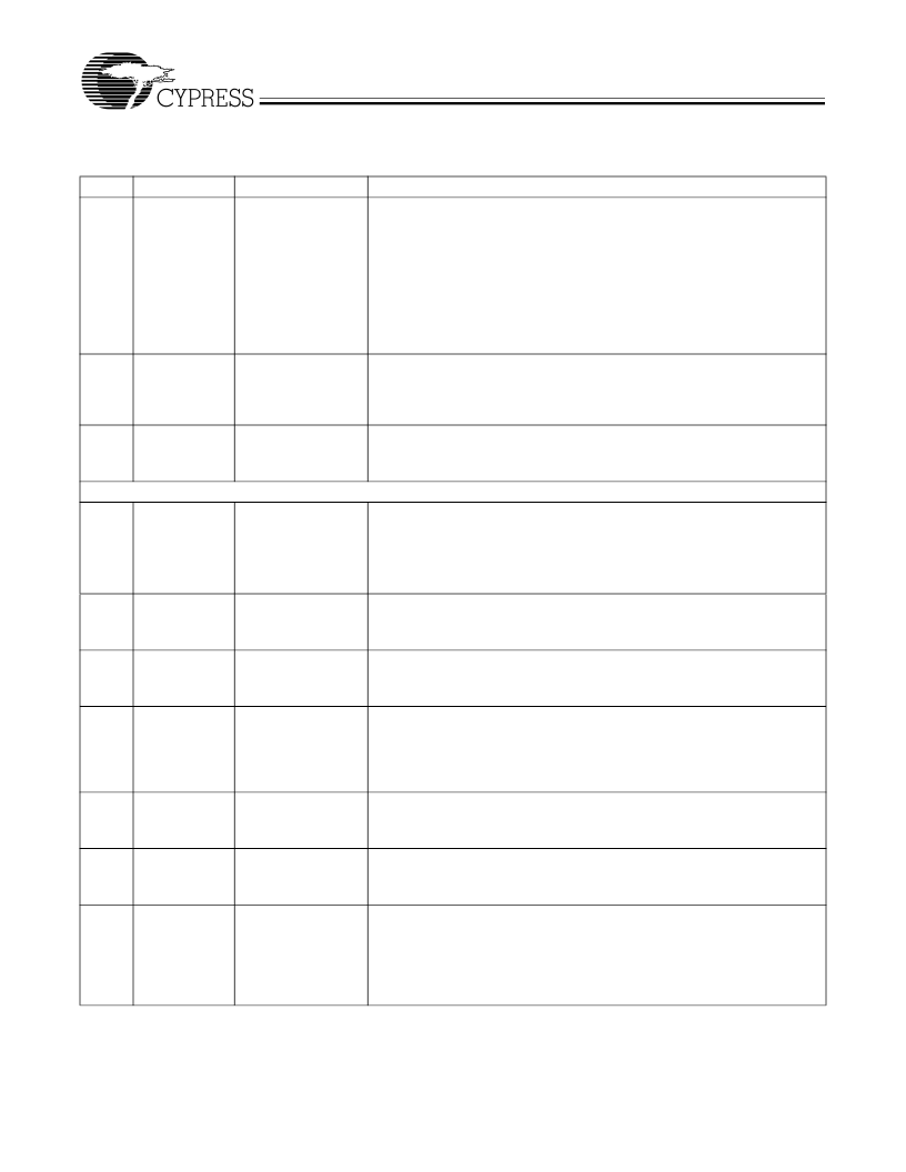
BYTE8/10*
Static control input
TTL levels
Normally wired HIGH
or LOW
Parallel Data Character Size Select.
Selects the input data character width. When BYTE8/10* is HIGH, the device
is in 8-bit mode. When BYTE8/10* is LOW, the part is in 10-bit mode. If the
encoder is enabled (ENCBYP* is HIGH), the data is encoded using the 8B/10B
code rules found in
Table 10
and
Table 11
.
When ENCBYP* is LOW, the part passes the 10 input bits (when BYTE8/10*
is HIGH) or 12 input bits (BYTE8/10* is LOW) directly to the serial stream
without encoding or decoding.
For affected pin groupings and function see
Table 1
and
Table 7
.
Global Logic Reset.
These inputs are pulsed LOW for one or more REFCLK periods to reset the
internal logic. They must be tied together or driven concurrently to ensure a
valid reset.
Factory Test Mode Select.
Used to force the part into a diagnostic test mode used for factory ATE test.
This pin is tied HIGH during normal operation.
52, 51
RESET*[1:0]
TTL input,
asynchronous
1
TEST*
TTL input,
asynchronous.
Normally wired HIGH
Analog I/O and Control
89, 90,
81, 82
OUTB
±
OUTA
±
PECL differential
outputs
Differential Serial Data Outputs.
These PECL compatible outputs are capable of driving terminated transmis-
sion lines or commercial fiber-optic transmitter modules.
An unused output pair may be powered down by leaving the outputs uncon-
nected and strapping the associated CURSETx pin to V
DD
.
Current-set Resistor Input for OUTA
±.
A precision resistor is connected between this input and a clean ground to set
the output differential amplitude and currents for the OUTA
±
differential driver.
Current-set Resistor Input for OUTB
±.
A precision resistor is connected between this input and a clean ground to set
the output differential amplitude and currents for the OUTB
±
differential driver.
Differential Serial Data Inputs.
These inputs accept the serial data stream for deserialization and decoding.
Only one serial stream at a time may be fed to the receiver PLL to extract the
data content. This stream is selected using the A/B* input. These inputs may
also be routed to the OUTB
±
serial outputs using the DLB[1:0] inputs.
Receive Data Input Selector.
Determines which internal or external serial bit-stream is passed to the receiv-
er clock and data recovery circuit. See
Table 3
for details.
Loop-back Select Inputs.
Selects connections between serial inputs and outputs. Controls diagnostic
loop-back and serial loop-through functions. See
Table 3
for details.
Carrier Detect Input.
Used to allow an external device to signify a valid signal is being presented to
the high speed PECL compatible input buffers, as is typical on an Optical
Module. When CARDET is deasserted LOW, the LFI
*
indicator asserts LOW
signifying a Link Fault. This input can be tied to V
DD
for copper media applica-
tions.
97
CURSETA
Analog input
78
CURSETB
Analog input
94, 93,
86, 85
INA
±
INB
±
PECL compatible
differential input
2
A/B*
TTL input,
asynchronous,
Internal Pull-Up
4,5
DLB[1:0]
TTL input,
asynchronous,
Internal Pull-Down
100
CARDET
PECL input,
asynchronous
Pin Descriptions
(continued)
CY7C924DX HOTLink Transceiver
Pin #
Name
I/O Characteristics
Signal Description
相關(guān)PDF資料 |
PDF描述 |
|---|---|
| CY7C954DX | ATM HOTLink Transceiver(ATM 熱接插收發(fā)器) |
| CY7C964A | Bus Interface Logic Circuit |
| CY7C964A-UM | Bus Interface Logic Circuit |
| CY7C964A-UMB | Bus Interface Logic Circuit |
| CY7C964A-ASC | Bus Interface Logic Circuit |
相關(guān)代理商/技術(shù)參數(shù) |
參數(shù)描述 |
|---|---|
| CY7C9335-270AC | 制造商:Cypress Semiconductor 功能描述:Descrambler/Framer Controller 100-Pin TQFP |
| CY7C9335A-270AXC | 功能描述:網(wǎng)絡(luò)控制器與處理器 IC SMPTE Decoder COM RoHS:否 制造商:Micrel 產(chǎn)品:Controller Area Network (CAN) 收發(fā)器數(shù)量: 數(shù)據(jù)速率: 電源電流(最大值):595 mA 最大工作溫度:+ 85 C 安裝風(fēng)格:SMD/SMT 封裝 / 箱體:PBGA-400 封裝:Tray |
| CY7C9335A-270AXCT | 功能描述:網(wǎng)絡(luò)控制器與處理器 IC SMPTE Decoder COM RoHS:否 制造商:Micrel 產(chǎn)品:Controller Area Network (CAN) 收發(fā)器數(shù)量: 數(shù)據(jù)速率: 電源電流(最大值):595 mA 最大工作溫度:+ 85 C 安裝風(fēng)格:SMD/SMT 封裝 / 箱體:PBGA-400 封裝:Tray |
| CY7C9528-BLC | 制造商:Cypress Semiconductor 功能描述:OC-12/3 (STM-4/1) FRAMER, 504 BGA - Bulk |
| CY7C9528-BLI | 制造商:Cypress Semiconductor 功能描述:OC-12/3 (STM-4/1) FRAMER, 504 BGA - Bulk |
發(fā)布緊急采購,3分鐘左右您將得到回復(fù)。