- 您現(xiàn)在的位置:買賣IC網(wǎng) > PDF目錄366550 > AM79C970AVCW (ADVANCED MICRO DEVICES INC) PCnet-PCI II Single-Chip Full-Duplex Ethernet Controller for PCI Local Bus Product PDF資料下載
參數(shù)資料
| 型號: | AM79C970AVCW |
| 廠商: | ADVANCED MICRO DEVICES INC |
| 元件分類: | 微控制器/微處理器 |
| 英文描述: | PCnet-PCI II Single-Chip Full-Duplex Ethernet Controller for PCI Local Bus Product |
| 中文描述: | 2 CHANNEL(S), 10M bps, LOCAL AREA NETWORK CONTROLLER, PQFP144 |
| 封裝: | TQFP-144 |
| 文件頁數(shù): | 176/219頁 |
| 文件大小: | 1065K |
| 代理商: | AM79C970AVCW |
第1頁第2頁第3頁第4頁第5頁第6頁第7頁第8頁第9頁第10頁第11頁第12頁第13頁第14頁第15頁第16頁第17頁第18頁第19頁第20頁第21頁第22頁第23頁第24頁第25頁第26頁第27頁第28頁第29頁第30頁第31頁第32頁第33頁第34頁第35頁第36頁第37頁第38頁第39頁第40頁第41頁第42頁第43頁第44頁第45頁第46頁第47頁第48頁第49頁第50頁第51頁第52頁第53頁第54頁第55頁第56頁第57頁第58頁第59頁第60頁第61頁第62頁第63頁第64頁第65頁第66頁第67頁第68頁第69頁第70頁第71頁第72頁第73頁第74頁第75頁第76頁第77頁第78頁第79頁第80頁第81頁第82頁第83頁第84頁第85頁第86頁第87頁第88頁第89頁第90頁第91頁第92頁第93頁第94頁第95頁第96頁第97頁第98頁第99頁第100頁第101頁第102頁第103頁第104頁第105頁第106頁第107頁第108頁第109頁第110頁第111頁第112頁第113頁第114頁第115頁第116頁第117頁第118頁第119頁第120頁第121頁第122頁第123頁第124頁第125頁第126頁第127頁第128頁第129頁第130頁第131頁第132頁第133頁第134頁第135頁第136頁第137頁第138頁第139頁第140頁第141頁第142頁第143頁第144頁第145頁第146頁第147頁第148頁第149頁第150頁第151頁第152頁第153頁第154頁第155頁第156頁第157頁第158頁第159頁第160頁第161頁第162頁第163頁第164頁第165頁第166頁第167頁第168頁第169頁第170頁第171頁第172頁第173頁第174頁第175頁當(dāng)前第176頁第177頁第178頁第179頁第180頁第181頁第182頁第183頁第184頁第185頁第186頁第187頁第188頁第189頁第190頁第191頁第192頁第193頁第194頁第195頁第196頁第197頁第198頁第199頁第200頁第201頁第202頁第203頁第204頁第205頁第206頁第207頁第208頁第209頁第210頁第211頁第212頁第213頁第214頁第215頁第216頁第217頁第218頁第219頁
AMD
P R E L I M I N A R Y
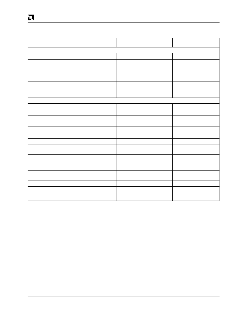
176
Am79C970A
DC CHARACTERISTICS over COMMERCIAL operating ranges unless otherwise
specified (continued)
Parameter
Symbol
Twisted Pair Interface (10BASE-T) (Continued)
V
RXDTH
RXD Switching Threshold
TXD
±
and TXP
±
Output HIGH Voltage
V
TXL
TXD
±
and TXP
±
Output LOW Voltage
V
TXI
TXD
±
and TXP
±
Differential
Output Voltage Imbalance
TXD
±
and TXP
±
Idle Output Voltage
R
TX
TXD
±
, TXP
±
Differential Driver
Output Impedance
Attachment Unit Interface (AUI)
Parameter Description
Test Conditions
Min
Max
Units
(Note 6)
–35
35
mV
V
TXH
AV
SS
= 0 V
AV
DD
–0.6
AV
DD
V
AV
DD
= 5 V
AV
SS
AV
SS
+0.6
V
–40
40
mV
V
TXOFF
40
mV
(Note 6)
80
I
IAXD
Input Current at DI+ and DI–
–1V < V
IN
< AV
DD
+ 0.5 V
–500
+500
μ
A
μ
A
mV
I
IAXC
Input Current at CI+ and CI–
–1V < V
IN
< AV
DD
+ 0.5 V
R
L
= 78
–500
+500
V
AOD
Differential Output Voltage
|(DO+)–(DO–)|
630
1200
V
AODOFF
Transmit Differential Output Idle Voltage
R
L
= 78
(Note 9)
R
L
= 78
(Note 8)
R
L
= 78
R
L
= 78
(Note 7)
–40
40
mV
I
AODOFF
Transmit Differential Output Idle Current
–1
1
mA
V
CMT
Transmit Output Common Mode Voltage
DO
±
Transmit Differential Output
Voltage Imbalance
Receive Data Differential Input Threshold
DI
±
and CI
±
Differential Input
Threshold (Squelch)
DI
±
and CI
±
Differential Mode Input
Voltage Range
DI
±
and CI
±
Input Bias Voltage
DO
±
Undershoot Voltage at ZERO
Differential on Transmit Return
to ZERO (ETD)
2.5
AV
DD
V
V
ODI
25
mV
V
ATH
–35
35
mV
V
ASQ
–275
–160
mV
V
IRDVD
–1.5
1.5
V
V
ICM
I
IN
= 0 mA
AV
DD
–3.0 AV
DD
–1.0
V
V
OPD
(Note 9)
–100
mV
Notes:
1. I
OL1
applies to AD[31:0], C/
BE
[3:0], PAR and
REQ
.
I
OL2
applies to
DEVSEL
,
FRAME
,
INTA
,
IRDY
,
PERR
,
SERR
,
STOP
,
TRDY
,
EECS ERA[7:0], ERACLK
,
EROE
,
DXCVR/
NOUT, ERD7/TXDAT, ERD6/TXEN and TDO.
I
OL3
applies to EESK/
LED1
/SFBD,
LED2
/SRDCLK, EEDO/
LED3
/SRD, and EEDI/
LNKST
.
2. V
OH
does not apply to open-drain output pins.
3. Outputs are CMOS and will be driven to rail if the load is not resistive.
4. I
IX
applies to all input pins except XTAL1.
5. I
OZL
and I
OZH
apply to all three-state output pins and bi-directional pins.
6. Parameter not tested. Value determined by characterization.
7. Tested, but to values in excess of limits. Test accuracy not sufficient to allow screening guard bands.
8. Correlated to other tested parameters—not tested directly.
9. Test not implemented to data sheet specification.
10. The power supply current in Magic Packet mode is linear. For example, at CLK = 20 MHz the maximum Magic Packet mode
power supply current would be 67 mA.
相關(guān)PDF資料 |
PDF描述 |
|---|---|
| AM79C970 | PCnetTM-PCI Single-Chip Ethernet Controller for PCI Local Bus |
| AM79C971VCW | PCnet⑩-FAST Single-Chip Full-Duplex 10/100 Mbps Ethernet Controller for PCI Local Bus |
| AM79C971 | PCnet⑩-FAST Single-Chip Full-Duplex 10/100 Mbps Ethernet Controller for PCI Local Bus |
| AM79C971KCW | IC LOGIC 16211 24-BIT FET BUS SWITCH -40+85C TSSOP-56 35/TUBE |
| AM79C972BKCW | PCnet⑩-FAST+ Enhanced 10/100 Mbps PCI Ethernet Controller with OnNow Support |
相關(guān)代理商/技術(shù)參數(shù) |
參數(shù)描述 |
|---|---|
| AM79C970AVI\\W | 制造商:Rochester Electronics LLC 功能描述:- Bulk |
| AM79C970AVI\W | 制造商:Rochester Electronics LLC 功能描述:- Bulk |
| AM79C970AVIW | 制造商:Rochester Electronics LLC 功能描述: |
| AM79C970AVW | 制造商:Rochester Electronics LLC 功能描述:- Bulk |
| AM79C970AWW WAF | 制造商:Advanced Micro Devices 功能描述: |
發(fā)布緊急采購,3分鐘左右您將得到回復(fù)。