- 您現(xiàn)在的位置:買賣IC網(wǎng) > PDF目錄98142 > SSTE32882HLBBKG (INTEGRATED DEVICE TECHNOLOGY INC) SSTE SERIES, PLL BASED CLOCK DRIVER, 4 TRUE OUTPUT(S), 0 INVERTED OUTPUT(S), PBGA176 PDF資料下載
參數(shù)資料
| 型號: | SSTE32882HLBBKG |
| 廠商: | INTEGRATED DEVICE TECHNOLOGY INC |
| 元件分類: | 時鐘及定時 |
| 英文描述: | SSTE SERIES, PLL BASED CLOCK DRIVER, 4 TRUE OUTPUT(S), 0 INVERTED OUTPUT(S), PBGA176 |
| 封裝: | 8 X 13.50 MM, 0.65 MM PITCH, GREEN, MO-246F, CABGA-176 |
| 文件頁數(shù): | 31/69頁 |
| 文件大小: | 1263K |
| 代理商: | SSTE32882HLBBKG |
第1頁第2頁第3頁第4頁第5頁第6頁第7頁第8頁第9頁第10頁第11頁第12頁第13頁第14頁第15頁第16頁第17頁第18頁第19頁第20頁第21頁第22頁第23頁第24頁第25頁第26頁第27頁第28頁第29頁第30頁當(dāng)前第31頁第32頁第33頁第34頁第35頁第36頁第37頁第38頁第39頁第40頁第41頁第42頁第43頁第44頁第45頁第46頁第47頁第48頁第49頁第50頁第51頁第52頁第53頁第54頁第55頁第56頁第57頁第58頁第59頁第60頁第61頁第62頁第63頁第64頁第65頁第66頁第67頁第68頁第69頁
1.25V/1.35V/1.5V REGISTERING CLOCK DRIVER WITH PARITY TEST AND QUAD CHIP SELECT
37
SSTE32882KA1
7314/5
CONFIDENTIAL - THE INFORMATION IN THIS DOCUMENT IS SUBJECT TO CHANGE WITHOUT NOTICE
SSTE32882KA1
1.25V/1.35V/1.5V REGISTERING CLOCK DRIVER WITH PARITY TEST AND QUAD CHIP SELECT
COMMERCIAL TEMPERATURE RANGE
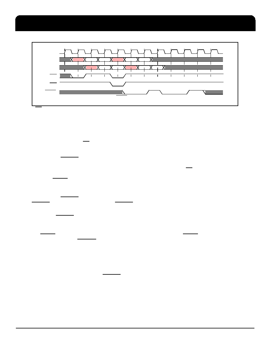
Parity-Error Occurrences During Control Word Programming
1 CK left out for better visibility.
POWER SAVING MODES
The device supports different power saving mechanisms.
When both inputs CK and CK are being held low the device stops operation and enters low-power static and
standby operation. It stops its PLL and floats all outputs except QACKE0, QACKE1, QBCKE0 and QBCKE1 which
are kept driven low. Before the device is taken out of standby operation by applying a stable input clock signal, the
register inputs DCS[n:0] must be pulled high to prevent accidential access to the control registers and DCKE0 as
well as DCKE1 must be pulled low for a certain period of time (tACT). The input clock must be stable for a time
(tSTAB) before any access to the device takes place. Stopping the clocks (CK = CK = low) will only put the
SSTE32882KA1 in low-power mode and will not clear the content of the control words. The control words will reset
only when RESET is diven low.
A float feature can be enabled by setting the corresponding bit in the control register. This causes the device to
monitor all the DCS[n:0] inputs and to float all outputs corresponding with the chip select gated inputs when all the
DCS[n:0] inputs are high. If any one of the DCS[n:0] inputs are low, the Qn outputs will function normally.
Once all the DCS[n;0] inputs are high, the gated address command inputs to the register can float to conserve input
termination power. DCKE0, DCKE1, DODT0 and DODT1 need to be driven by the system all the time.
The RESET input has priority over all other power saving mechanisms. When RESET is driven low, it will force the
Qn outputs to float, the ERROUT output high, the QACKE0, QACKE1, QBCKE0 and QBCKE1 outputs low, and
disables Input Bus Termination (IBT).
REGISTER CKE POWER DOWN
If RC9[DBA1] is set to “1”, the SSTE32882KA1 monitors both DCKEn input signals and enters into power saving
state when it latches Low on both DCKEn inputs and at least one of the DCKEn input has transitioned from High to
Low. If any input Chip Select signal (DCS[n:0]) is asserted together with DCKEn, the SSTE32882KA1 transfers the
corresponding command to its outputs together with QxCKEn Low.
There are two modes of CKE Power Down selected by RC9. Bit DBA0 in RC9 indicates whether the register turns
off IBT or keeps IBT on.
CK(1)
CA
Input
PAR_IN
CA0
P0
CA1
P1
CA2
P2
ERROUT
n
n+1
n+2
n+3
n+4
n+5
n+6
ERROUTresulting from CA0 - P0, followed by 2nd error during control word access in CA3 - P3
n+7
n+8
n+9
CA3
P3
P4
CA4
CA5
P5
DCS0
DCS1
相關(guān)PDF資料 |
PDF描述 |
|---|---|
| SSTUA32864EC,557 | SSTU SERIES, POSITIVE EDGE TRIGGERED D FLIP-FLOP, TRUE OUTPUT, PBGA96 |
| SSTUA32866EC/G | 32866 SERIES, POSITIVE EDGE TRIGGERED D FLIP-FLOP, COMPLEMENTARY OUTPUT, PBGA96 |
| SSTUA32866EC,557 | 32866 SERIES, POSITIVE EDGE TRIGGERED D FLIP-FLOP, COMPLEMENTARY OUTPUT, PBGA96 |
| SSTUA32866EC/G,551 | 32866 SERIES, POSITIVE EDGE TRIGGERED D FLIP-FLOP, COMPLEMENTARY OUTPUT, PBGA96 |
| SSTUA32866EC/G,557 | 32866 SERIES, POSITIVE EDGE TRIGGERED D FLIP-FLOP, COMPLEMENTARY OUTPUT, PBGA96 |
相關(guān)代理商/技術(shù)參數(shù) |
參數(shù)描述 |
|---|---|
| SSTE32882HLBBKG8 | 制造商:Integrated Device Technology Inc 功能描述:Registering Clock Driver 176-Pin CABGA T/R 制造商:Integrated Device Technology Inc 功能描述:176 BGA (GREEN) - Tape and Reel 制造商:Integrated Device Technology Inc 功能描述:DDR3 LV REGISTER |
| SSTE32882KA1AKG | 功能描述:寄存器 RoHS:否 制造商:NXP Semiconductors 邏輯類型:CMOS 邏輯系列:HC 電路數(shù)量:1 最大時鐘頻率:36 MHz 傳播延遲時間: 高電平輸出電流:- 7.8 mA 低電平輸出電流:7.8 mA 電源電壓-最大:6 V 最大工作溫度:+ 125 C 封裝 / 箱體:SOT-38 封裝:Tube |
| SSTE32882KA1AKG8 | 功能描述:寄存器 RoHS:否 制造商:NXP Semiconductors 邏輯類型:CMOS 邏輯系列:HC 電路數(shù)量:1 最大時鐘頻率:36 MHz 傳播延遲時間: 高電平輸出電流:- 7.8 mA 低電平輸出電流:7.8 mA 電源電壓-最大:6 V 最大工作溫度:+ 125 C 封裝 / 箱體:SOT-38 封裝:Tube |
| SSTE32882KA1AKG8/M | 制造商:Integrated Device Technology Inc 功能描述:DDR3 REGISTER - Tape and Reel |
| SSTE32882TNA1AKG8 | 制造商:Integrated Device Technology Inc 功能描述:DDR3 REGISTER - Tape and Reel |
發(fā)布緊急采購,3分鐘左右您將得到回復(fù)。