- 您現(xiàn)在的位置:買賣IC網(wǎng) > PDF目錄98142 > SSTE32882HLBAKG (INTEGRATED DEVICE TECHNOLOGY INC) SSTE SERIES, PLL BASED CLOCK DRIVER, 4 TRUE OUTPUT(S), 0 INVERTED OUTPUT(S), PBGA176 PDF資料下載
參數(shù)資料
| 型號(hào): | SSTE32882HLBAKG |
| 廠商: | INTEGRATED DEVICE TECHNOLOGY INC |
| 元件分類: | 時(shí)鐘及定時(shí) |
| 英文描述: | SSTE SERIES, PLL BASED CLOCK DRIVER, 4 TRUE OUTPUT(S), 0 INVERTED OUTPUT(S), PBGA176 |
| 封裝: | 8 X 13.50 MM, 0.65 MM PITCH, GREEN, MO-246F, CABGA-176 |
| 文件頁(yè)數(shù): | 49/69頁(yè) |
| 文件大小: | 1263K |
| 代理商: | SSTE32882HLBAKG |
第1頁(yè)第2頁(yè)第3頁(yè)第4頁(yè)第5頁(yè)第6頁(yè)第7頁(yè)第8頁(yè)第9頁(yè)第10頁(yè)第11頁(yè)第12頁(yè)第13頁(yè)第14頁(yè)第15頁(yè)第16頁(yè)第17頁(yè)第18頁(yè)第19頁(yè)第20頁(yè)第21頁(yè)第22頁(yè)第23頁(yè)第24頁(yè)第25頁(yè)第26頁(yè)第27頁(yè)第28頁(yè)第29頁(yè)第30頁(yè)第31頁(yè)第32頁(yè)第33頁(yè)第34頁(yè)第35頁(yè)第36頁(yè)第37頁(yè)第38頁(yè)第39頁(yè)第40頁(yè)第41頁(yè)第42頁(yè)第43頁(yè)第44頁(yè)第45頁(yè)第46頁(yè)第47頁(yè)第48頁(yè)當(dāng)前第49頁(yè)第50頁(yè)第51頁(yè)第52頁(yè)第53頁(yè)第54頁(yè)第55頁(yè)第56頁(yè)第57頁(yè)第58頁(yè)第59頁(yè)第60頁(yè)第61頁(yè)第62頁(yè)第63頁(yè)第64頁(yè)第65頁(yè)第66頁(yè)第67頁(yè)第68頁(yè)第69頁(yè)
1.25V/1.35V/1.5V REGISTERING CLOCK DRIVER WITH PARITY TEST AND QUAD CHIP SELECT
53
SSTE32882KA1
7314/5
CONFIDENTIAL - THE INFORMATION IN THIS DOCUMENT IS SUBJECT TO CHANGE WITHOUT NOTICE
SSTE32882KA1
1.25V/1.35V/1.5V REGISTERING CLOCK DRIVER WITH PARITY TEST AND QUAD CHIP SELECT
COMMERCIAL TEMPERATURE RANGE
A or B output disable allows the use of the SSTE32882KA1 in reduced parts count applications such as DDR3
Mini-RDIMMs. When output disable is asserted, all outputs on the corresponding side of the register, including the
clock drivers, remain in Hi-Z at all times. When RC0[DBA0] = 1, all A-side Q-outputs and Y1 and Y3 outputs will be
disabled. When RC0[DBA1] = 1, all B-side Q-outputs and Y0 and Y2 outputs will be disabled. When RC0[DBA0] =
1 and RC0[DBA1] = 1, all A-side and B-side Q-outputs and Yn outputs will be disabled.
RC1: Clock Driver Enable Control Word
Output clocks may be individually turned on or off to conserve power. The system must read the module SPD to
determine which clock outputs are used by the module. The PLL remains locked on CK/CK unless the system
stops the clock inputs to the SSTE32882KA1 to enter the lowest power mode.
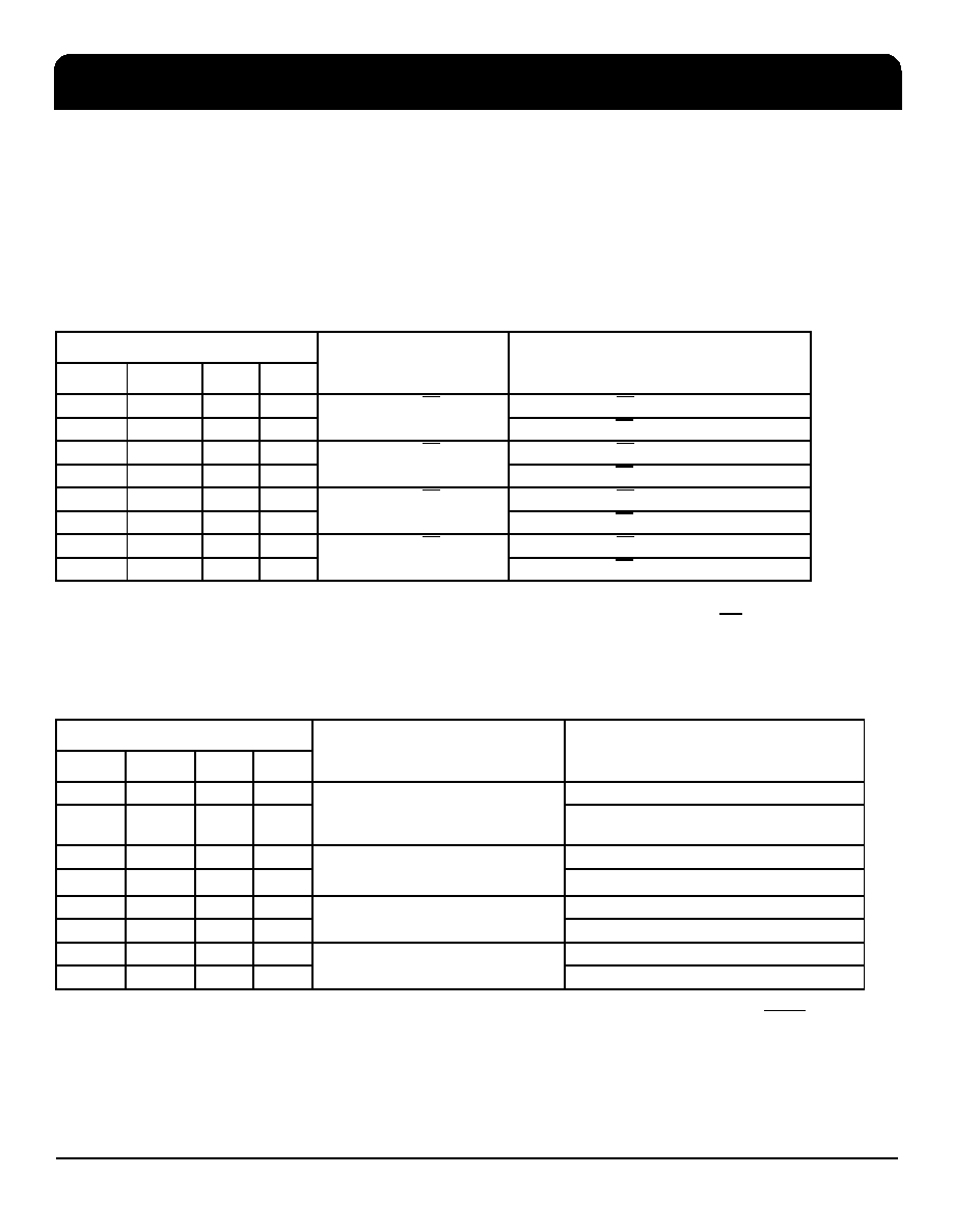
RC2: Timing Control Word
Input
Definition
Encoding
DBA1
DBA0
DA4
DA3
x
0
Disable Y0/Y0 clock
Y0/Y0 clock enabled
xx
x
1
Y0/Y0 clock disabled
x
0
x
Disable Y1/Y1 clock
Y1/Y1 clock enabled
xx
1
x
Y1/Y1 clock disabled
x
0
x
Disable Y2/Y2 clock
Y2/Y2 clock enabled
x1
x
Y2/Y2 clock disabled
0
x
Disable Y3/Y3 clock
Y3/Y3 clock enabled
1x
x
Y3/Y3 clock disabled
Input
Definition
Encoding
DBA1
DBA0
DA4
DA3
xx
x
0
Address- and command-nets
pre-launch (Control Signals QxCKE,
QxCS, QxODT do not apply)
Standard (1/2 Clock)
x
1
Address and command nets pre-launch (3/4
Clock)
xx
0
x
1T/3T Output timing
1T timing
xx
1
x
3T timing(1)
1
There is no floating once 3T timing is activated.
x0
x
Input Bus Termination(2)
2
If MIRROR is ‘HIGH’ then Input Bus Termination (IBT) is turned off, or on all inputs except the DCSn and
DODTn inputs.
100
Ω
x
1
x
150
Ω
0x
x
Frequency Band Select
Operation (Frequency Band 1)
1
x
Test Mode (Frequency Band 2)
相關(guān)PDF資料 |
PDF描述 |
|---|---|
| SSTE32882HLBBKG | SSTE SERIES, PLL BASED CLOCK DRIVER, 4 TRUE OUTPUT(S), 0 INVERTED OUTPUT(S), PBGA176 |
| SSTUA32864EC,557 | SSTU SERIES, POSITIVE EDGE TRIGGERED D FLIP-FLOP, TRUE OUTPUT, PBGA96 |
| SSTUA32866EC/G | 32866 SERIES, POSITIVE EDGE TRIGGERED D FLIP-FLOP, COMPLEMENTARY OUTPUT, PBGA96 |
| SSTUA32866EC,557 | 32866 SERIES, POSITIVE EDGE TRIGGERED D FLIP-FLOP, COMPLEMENTARY OUTPUT, PBGA96 |
| SSTUA32866EC/G,551 | 32866 SERIES, POSITIVE EDGE TRIGGERED D FLIP-FLOP, COMPLEMENTARY OUTPUT, PBGA96 |
相關(guān)代理商/技術(shù)參數(shù) |
參數(shù)描述 |
|---|---|
| SSTE32882HLBAKG8 | 功能描述:寄存器 DDR3 LV REGISTER RoHS:否 制造商:NXP Semiconductors 邏輯類型:CMOS 邏輯系列:HC 電路數(shù)量:1 最大時(shí)鐘頻率:36 MHz 傳播延遲時(shí)間: 高電平輸出電流:- 7.8 mA 低電平輸出電流:7.8 mA 電源電壓-最大:6 V 最大工作溫度:+ 125 C 封裝 / 箱體:SOT-38 封裝:Tube |
| SSTE32882HLBAKG8/M | 制造商:Integrated Device Technology Inc 功能描述:IC, REG 32882_LV D3-1600 176TFBGA GRN - Tape and Reel |
| SSTE32882HLBBKG | 制造商:Integrated Device Technology Inc 功能描述:Registering Clock Driver 176-Pin CABGA Tray 制造商:Integrated Device Technology Inc 功能描述:176 BGA (GREEN) - Bulk 制造商:Integrated Device Technology Inc 功能描述:DDR3 LV REGISTER |
| SSTE32882HLBBKG8 | 制造商:Integrated Device Technology Inc 功能描述:Registering Clock Driver 176-Pin CABGA T/R 制造商:Integrated Device Technology Inc 功能描述:176 BGA (GREEN) - Tape and Reel 制造商:Integrated Device Technology Inc 功能描述:DDR3 LV REGISTER |
| SSTE32882KA1AKG | 功能描述:寄存器 RoHS:否 制造商:NXP Semiconductors 邏輯類型:CMOS 邏輯系列:HC 電路數(shù)量:1 最大時(shí)鐘頻率:36 MHz 傳播延遲時(shí)間: 高電平輸出電流:- 7.8 mA 低電平輸出電流:7.8 mA 電源電壓-最大:6 V 最大工作溫度:+ 125 C 封裝 / 箱體:SOT-38 封裝:Tube |
發(fā)布緊急采購(gòu),3分鐘左右您將得到回復(fù)。