- 您現(xiàn)在的位置:買賣IC網(wǎng) > PDF目錄373367 > SC1200 (Texas Instruments, Inc.) Precision Analog-to-Digital Converter (ADC) and Digital-to-Analog Converter (DAC) with 8051 Microcontroller and Flash Memory PDF資料下載
參數(shù)資料
| 型號: | SC1200 |
| 廠商: | Texas Instruments, Inc. |
| 英文描述: | Precision Analog-to-Digital Converter (ADC) and Digital-to-Analog Converter (DAC) with 8051 Microcontroller and Flash Memory |
| 中文描述: | 精密模擬到數(shù)字轉(zhuǎn)換器(ADC)和數(shù)字到模擬轉(zhuǎn)換器(DAC)的8051微控制器和閃存 |
| 文件頁數(shù): | 17/60頁 |
| 文件大小: | 802K |
| 代理商: | SC1200 |
第1頁第2頁第3頁第4頁第5頁第6頁第7頁第8頁第9頁第10頁第11頁第12頁第13頁第14頁第15頁第16頁當(dāng)前第17頁第18頁第19頁第20頁第21頁第22頁第23頁第24頁第25頁第26頁第27頁第28頁第29頁第30頁第31頁第32頁第33頁第34頁第35頁第36頁第37頁第38頁第39頁第40頁第41頁第42頁第43頁第44頁第45頁第46頁第47頁第48頁第49頁第50頁第51頁第52頁第53頁第54頁第55頁第56頁第57頁第58頁第59頁第60頁
MSC1200
SBAS289E
17
www.ti.com
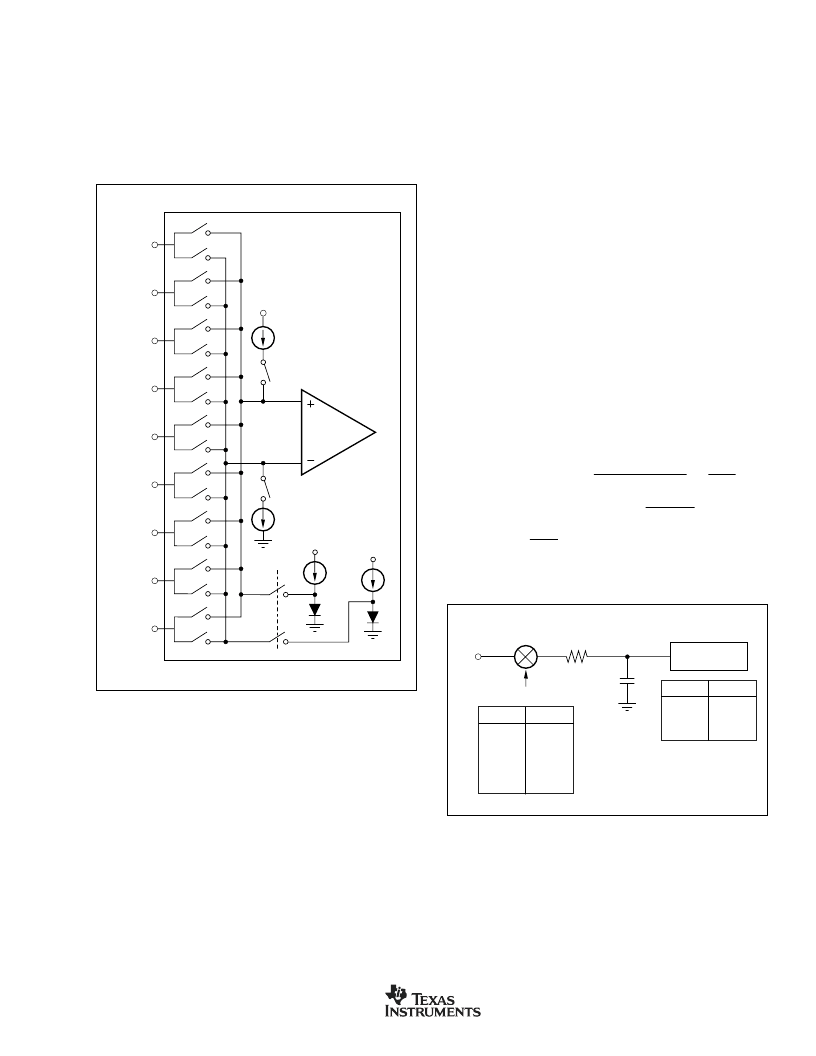
FIGURE 6. Input Multiplexer Configuration.
FIGURE 7. Analog Input Structure (without buffer).
INPUT MULTIPLEXER
The input multiplexer provides for any combination of differential
inputs to be selected as the input channel, as shown in Figure 6.
If AIN0 is selected as the positive differential input channel, any
other channel can be selected as the negative differential input
channel. With this method, it is possible to have up to eight fully
differential input channels. It is also possible to switch the polarity
of the differential input pair to negate any offset voltages.
In addition, current sources are supplied that will source or
sink current to detect open or short circuits on the pins.
TEMPERATURE SENSOR
On-chip diodes provide temperature sensing capability. When
the configuration register for the input MUX is set to all 1s,
the diodes are connected to the input of the ADC. All other
channels are open.
BURNOUT DETECT
When the Burnout Detect (BOD) bit is set in the ADC control
configuration register (ADCON0 DC
H
), two current sources are
enabled. The current source on the positive input channel sources
approximately 2
μ
A of current. The current source on the negative
input channel sinks approximately 2
μ
A. This allows for the
detection of an open circuit (full-scale reading) or short circuit
(small differential reading) on the selected input differential pair.
Enabling the buffer is recommended when BOD is enabled.
INPUT BUFFER
The analog input impedance is always high, regardless of
PGA setting (when the buffer is enabled). With the buffer
enabled, the input voltage range is reduced and the analog
power-supply current is higher. If the limitation of input
voltage range is acceptable, then the buffer is always pre-
ferred.
The input impedance of the MSC1200 without the buffer
is 7M
/PGA. The buffer is controlled by the state of the BUF
bit in the ADC control register (ADCON0 DC
H
).
ANALOG INPUT
When the buffer is not selected, the input impedance of the
analog input changes with ACLK clock frequency (ACLK
F6
H
) and gain (PGA). The relationship is:
A
pedance
MHz
ACLK Frequency
M
PGA
IN
Im
( )
1
7
where ACLK frequency (f
ACLK
) =
f
ACLK
64
f
ACLK
CLK
+
1
and f
MOD
=
.
Figure 7 shows the basic input structure of the MSC1200.
R
SWITCH
(3k
Sampling Frequency = f
SAMP
High Impedance
> 1G
C
S
AGND
A
IN
PGA
f
SAMP
f
MOD
2
×
f
MOD
4
×
f
MOD
8
×
f
MOD
16
×
f
MOD
1, 2, 4
8
16
32
64, 128
PGA
C
S
9pF
18pF
36pF
1
2
4 to 128
AIN3
AIN4
AIN5
AIN6
AIN0
AIN1
AIN2
AIN7
AINCOM
Burnout Detect (2
μ
A)
Burnout Detect (2
μ
A)
Temperature Sensor
AV
DD
AGND
Buffer
I
80
I
AV
DD
AV
DD
In+
In
–
相關(guān)PDF資料 |
PDF描述 |
|---|---|
| SC141E | 6-A AND 10-A SILICON TRIACS |
| SC146B | 6-A AND 10-A SILICON TRIACS |
| SC141B | 6-A AND 10-A SILICON TRIACS |
| SC141D | 6-A AND 10-A SILICON TRIACS |
| SC141M | 6-A AND 10-A SILICON TRIACS |
相關(guān)代理商/技術(shù)參數(shù) |
參數(shù)描述 |
|---|---|
| SC12-00 | 制造商: 功能描述: 制造商:undefined 功能描述: |
| SC1-200/5A | 制造商:TE Connectivity 功能描述:CURRENT TRANSFORMER CASE SIZE 1 SPLIT CORE 200/5 AMPS AC 1.5VA-CL1 2.5VA-CL3 |
| SC1200/KR32A | 制造商:X-10 Pro 功能描述:Personal Assistance Voice Dialer |
| SC12004 | 制造商:Ferraz Shawmut 功能描述: |
| SC1200UCL-266 | 制造商:Rochester Electronics LLC 功能描述: |
發(fā)布緊急采購,3分鐘左右您將得到回復(fù)。