- 您現(xiàn)在的位置:買賣IC網(wǎng) > PDF目錄385641 > MT9LD272 (Micron Technology, Inc.) 2Meg x 72 Buffered DRAM DIMMs(2M x 72緩沖動(dòng)態(tài)RAM模塊(雙列直插存儲(chǔ)器模塊)) PDF資料下載
參數(shù)資料
| 型號(hào): | MT9LD272 |
| 廠商: | Micron Technology, Inc. |
| 英文描述: | 2Meg x 72 Buffered DRAM DIMMs(2M x 72緩沖動(dòng)態(tài)RAM模塊(雙列直插存儲(chǔ)器模塊)) |
| 中文描述: | 2Meg × 72緩沖內(nèi)存插槽(200萬× 72緩沖動(dòng)態(tài)內(nèi)存模塊(雙列直插存儲(chǔ)器模塊)) |
| 文件頁數(shù): | 1/29頁 |
| 文件大?。?/td> | 491K |
| 代理商: | MT9LD272 |
當(dāng)前第1頁第2頁第3頁第4頁第5頁第6頁第7頁第8頁第9頁第10頁第11頁第12頁第13頁第14頁第15頁第16頁第17頁第18頁第19頁第20頁第21頁第22頁第23頁第24頁第25頁第26頁第27頁第28頁第29頁
2, 4 Meg x 72 Buffered DRAM DIMMs
DM33.p65 – Rev. 2/99
Micron Technology, Inc., reserves the right to change products or specifications without notice.
1999, Micron Technology, Inc.
1
2, 4 MEG x 72
BUFFERED DRAM DIMMs
OBSOLETE
DRAM
MODULE
MT9LD272(X), MT18LD472(F)(X)
For the latest data sheet, please refer to the Micron Web
site:
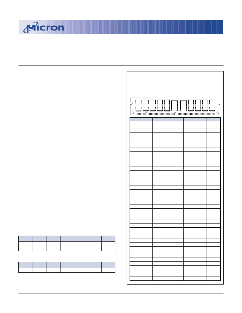
PIN ASSIGNMENT (Front View )PIN
1
2
3
4
5
6
7
8
9
10
11
12
13
14
15
16
17
18
19
20
21
22
23
24
25
26
27
28
29
30
31
32
33
34
35
36
37
38
39
40
41
42
SYMBOL
V
SS
DQ0
DQ1
DQ2
DQ3
V
DD
DQ4
DQ5
DQ6
DQ7
DQ8
V
SS
DQ9
DQ10
DQ11
DQ12
DQ13
V
DD
DQ14
DQ15
DQ16
DQ17
V
SS
NC
NC
V
DD
WE0#
CAS0#
RFU
RAS0#
OE0#
V
SS
A0
A2
A4
A6
A8
A10
NC (A12)
V
DD
RFU
RFU
PIN
43
44
45
46
47
48
49
50
51
52
53
54
55
56
57
58
59
60
61
62
63
64
65
66
67
68
69
70
71
72
73
74
75
76
77
78
79
80
81
82
83
84
SYMBOL
V
SS
OE2#
RAS2#
CAS4#
RFU
WE2#
V
DD
NC
NC
DQ18
DQ19
V
SS
DQ20
DQ21
DQ22
DQ23
V
DD
DQ24
RFU
RFU
RFU
RFU
DQ25
DQ26
DQ27
V
SS
DQ28
DQ29
DQ30
DQ31
V
DD
DQ32
DQ33
DQ34
DQ35
V
SS
PD1
PD3
PD5
PD7
ID0
V
DD
PIN
85
86
87
88
89
90
91
92
93
94
95
96
97
98
99
100
101
102
103
104
105
106
107
108
109
110
111
112
113
114
115
116
117
118
119
120
121
122
123
124
125
126
SYMBOL
V
SS
DQ36
DQ37
DQ38
DQ39
V
DD
DQ40
DQ41
DQ42
DQ43
DQ44
V
SS
DQ45
DQ46
DQ47
DQ48
DQ49
V
DD
DQ50
DQ51
DQ52
DQ53
V
SS
NC
NC
V
DD
RFU
NC
RFU
NC
RFU
V
SS
A1
A3
A5
A7
A9
A11
NC (A13)
V
DD
RFU
B0
PIN
127
128
129
130
131
132
133
134
135
136
137
138
139
140
141
142
143
144
145
146
147
148
149
150
151
152
153
154
155
156
157
158
159
160
161
162
163
164
165
166
167
168
SYMBOL
V
SS
RFU
NC
NC
RFU
PDE#
V
DD
NC
NC
DQ54
DQ55
V
SS
DQ56
DQ57
DQ58
DQ59
V
DD
DQ60
RFU
RFU
RFU
RFU
DQ61
DQ62
DQ63
V
SS
DQ64
DQ65
DQ66
DQ67
V
DD
DQ68
DQ69
DQ70
DQ71
V
SS
PD2
PD4
PD6
PD8
ID1
V
DD
FEATURES
JEDEC-standard ECC pinout in a 168-pin, dual in-
line memory module (DIMM)
16MB (2 Meg x 72) and 32MB (4 Meg x 72)
High-performance CMOS silicon-gate process
Single +3.3V ±0.3V power supply
All inputs, outputs and clocks are TTL-compatible
Refresh modes: RAS#-ONLY, CAS#-BEFORE- RAS#
(CBR) and HIDDEN
All inputs are buffered except RAS#
2,048 cycles (11 row, 11 column addresses) or
4,096 cycles (12 row, 10 column addresses)
FAST-PAGE-MODE (FPM) or Extended Data-Out
(EDO) PAGE MODE access cycles
OPTIONS
Package
168-pin DIMM (gold)
MARKING
G
Timing
50ns access
60ns access
-5*
-6
Access Cycles
FAST PAGE MODE
EDO PAGE MODE
None
X
Refresh
2,048 cycles across 32ms
4,096 cycles across 64ms (32MB only)
None
F
* EDO version only
168-Pin DIMM
NOTE:
Pin symbols in parentheses are not used on these modules but
may be used for other modules in this product family. They are
for reference only.
KEY TIMING PARAMETERS
EDO Operating Mode
SPEED
-5
-6
t
RC
84ns
104ns
t
RAC
50ns
60ns
t
PC
20ns
25ns
t
AA
30ns
35ns
t
CAC
18ns
20ns
t
CAS
8ns
10ns
FPM Operating Mode
SPEED
-6
t
RC
110ns
t
RAC
60ns
t
PC
35ns
t
AA
35ns
t
CAC
20ns
t
RP
40ns
相關(guān)PDF資料 |
PDF描述 |
|---|---|
| MT9VDDT1672A | DDR SDRAM DIMM |
| MT9VDDT3272A | DDR SDRAM DIMM |
| MTB2P50E | Power MOSFET 2 Amps, 500 Volts(2A, 500V功率MOSFET) |
| MTB50P03HDL | Power MOSFET 50 Amps, 30 Volts, Logic Level(50A, 30V, D2PAK, P溝道功率MOSFET) |
| MTD20N06HDLT4 | Power MOSFET 20 Amps, 60 Volts, Logic Level N−Channel DPAK |
相關(guān)代理商/技術(shù)參數(shù) |
參數(shù)描述 |
|---|---|
| MT9LD272A | 制造商:MICRON 制造商全稱:Micron Technology 功能描述:2, 4 MEG x 72 NONBUFFERED DRAM DIMMs |
| MT9LD272AG-52B | 制造商:未知廠家 制造商全稱:未知廠家 功能描述:x72 Burst EDO Page Mode DRAM Module |
| MT9LD272AG-5X | 制造商:未知廠家 制造商全稱:未知廠家 功能描述:x72 EDO Page Mode DRAM Module |
| MT9LD272AG-6 | 制造商:未知廠家 制造商全稱:未知廠家 功能描述:x72 Fast Page Mode DRAM Module |
| MT9LD272AG-60B | 制造商:未知廠家 制造商全稱:未知廠家 功能描述:x72 Burst EDO Page Mode DRAM Module |
發(fā)布緊急采購,3分鐘左右您將得到回復(fù)。