- 您現(xiàn)在的位置:買賣IC網(wǎng) > PDF目錄371014 > MC145225 (Motorola, Inc.) Dual PLL Frequency Synthesizers With DACs and Voltage Multipliers(帶DACs和電壓乘法器的雙PLL頻率合成器) PDF資料下載
參數(shù)資料
| 型號: | MC145225 |
| 廠商: | Motorola, Inc. |
| 英文描述: | Dual PLL Frequency Synthesizers With DACs and Voltage Multipliers(帶DACs和電壓乘法器的雙PLL頻率合成器) |
| 中文描述: | 雙鎖相環(huán)頻率合成器與DAC和電壓倍增器(帶數(shù)模轉(zhuǎn)換器和電壓乘法器的雙鎖相環(huán)頻率合成器) |
| 文件頁數(shù): | 57/71頁 |
| 文件大?。?/td> | 906K |
| 代理商: | MC145225 |
第1頁第2頁第3頁第4頁第5頁第6頁第7頁第8頁第9頁第10頁第11頁第12頁第13頁第14頁第15頁第16頁第17頁第18頁第19頁第20頁第21頁第22頁第23頁第24頁第25頁第26頁第27頁第28頁第29頁第30頁第31頁第32頁第33頁第34頁第35頁第36頁第37頁第38頁第39頁第40頁第41頁第42頁第43頁第44頁第45頁第46頁第47頁第48頁第49頁第50頁第51頁第52頁第53頁第54頁第55頁第56頁當(dāng)前第57頁第58頁第59頁第60頁第61頁第62頁第63頁第64頁第65頁第66頁第67頁第68頁第69頁第70頁第71頁

MC145225 MC145230
57
MOTOROLA RF/IF DEVICE DATA
7E. VOLTAGE MULTIPLIER STALL AVOIDANCE
There are three important criteria to note, highlighted in
the following sections:
Allowing for Voltage Build,
Ensuring Valid Counter Programming,
and
Allowing for
Overshoot.
Violation of any of these may cause the voltage
multiplier to collapse. Once the voltage collapses, the loop
goes out of lock and can not recover until the voltage is
allowed to build up again. For an active loop, the voltage
multiplier is designed to maintainthe multiplied voltage on the
phase/frequency detector supply pin (Cmult). If the main loop
is active, the multiplier cannot build the voltage.
Allowing for Voltage Build
After power up, a sufficient time interval must be provided
for the on–chip voltage multiplier to build up the voltage on
the Cmult pin. During this interval, the phase/frequency
detector outputs for the main loop (PDout–Hi and PDout–Lo)
must be inactive (floating outputs). The POR (power–on
reset) circuit forces this “float” condition, thus allowing the
voltage to build on the Cmult pin.
The duration of the interval to build the voltage is
determined by the external capacitor size tied to the Cmult pin
and the charging current which is 100
μ
A minimum. The
following formula may be used:
T = CV/I
where
T is the interval in seconds,
C is the Cmult capacitor size in farads,
V is the desired voltage on Cmult in volts, and
I is the charging current, 1 x 10
–4
amps.
The desired voltage on Cmult is 4 V for a nominal 2 V
supply and 5 V for any supply above 2.6 V.
After this interval, the chip can maintain the voltage on the
Cmult pin and the phase detectors may be safely placed in the
active state.
The interval above also applies when the voltage multiplier
is turned off (with power applied) via bits R 19 R 18 R 17
being 000. After the multiplier is turned back on, sufficient
time must be allowed for the voltage to build on Cmult. In this
case, typically an external resistor does not allow the Cmult
voltage to discharge below approximately Vpos (see Section
5E, under
Cmult)
. Note that if the voltage multiplier is NOT
turned off (that is, the above bits are unequal to 000), the
keep–alive circuit maintains the multiplied voltage on Cmult.
Ensuring Valid Counter Programming
Before the PLLs and/or phase detectors are taken out of
standby, legitimate divide ratios (pertinent to the application)
must be loaded in the registers. For example, proper divide
ratios must be loaded for the R, N, R , and N counters. Also,
proper values for all other bits must be loaded. For example:
selection of crystal or external reference mode must be made
prior to activation of the loops.
After the IC is initialized with the proper bits loaded, the
main loop may then be safely activated via the phase
detector float bit and/or the PLL standby bit being
programmed to 0.
Allowing for Overshoot
The VCO control voltage overshoot for the main loop must
not be allowed to exceed the capability of the phase/
frequency detectors’ maximum output voltage. The
detectors’ maximum output voltage is determined by the
minimum voltage at Cmult and the headroom required for the
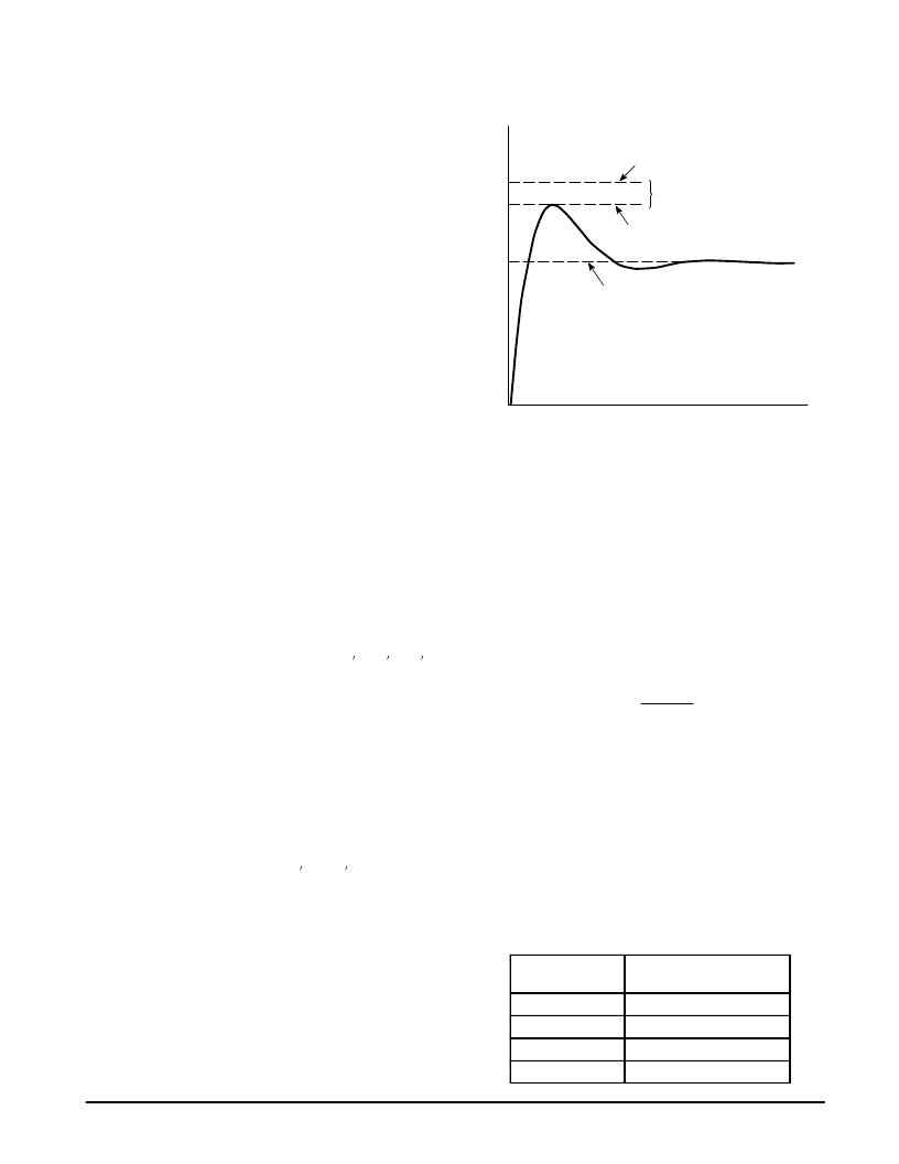
current source. See the following figure.
Steady–state Control Voltage
V
Voltage at Cmult Pin
Headroom for Current Source
Overshoot
Time
For example, if the main supply voltage (Vpos) is 3 V and
the voltage multiplier is utilized, the minimum voltage at Cmult
is 4.75 V. Then, to allow for current source headroom, the
maximum output voltage from the parameter table in Section
3C is approximately Cmult – 0.6 V or 4.2 V approximately.
Thus, the maximum output overshoot voltage at the
phase/frequency detector outputs should be no more than
4.2 V.
Continuing the above example, if the loop is designed with
20% overshoot in the VCO control voltage, then the
overshoot must be subtracted off of the 4.2 V shown above.
Therefore, the upper end of the control voltage to the VCO
must be no more than approximately 3.64 V.
The equations below can be used to determine
constraints:
V
φ
– 1.2
2
α
+ 1
V
≤
SSVmax = V
φ
–
α
(
V) – 0.6
where
V is the VCO control voltage range, the maximum minus
the minimum voltage,
V
φ
is the minimum phase detector supply voltage (at the
Cmult pin) per the following table,
α
is the control voltage overshoot in decimal; for example,
20% overshoot is 0.2, and
SSVmax is the maximum allowed steady–state VCO
control voltage.
MINIMUM PHASE DETECTOR VOLTAGE
FROM VOLTAGE MULTIPLIER
Supply Voltage,
Vpos
Minimum Phase Detector
Voltage, V
φ
3.32 V
1.8 V
2.0 V
3.72 V
2.5 V
4.75 V
3.6 V
4.75 V
相關(guān)PDF資料 |
PDF描述 |
|---|---|
| MC145230 | Dual PLL Frequency Synthesizers With DACs and Voltage Multipliers(帶DACs和電壓乘法器的雙PLL頻率合成器) |
| MC14528BCL | Dual Monostable Multivibrator |
| MC14528 | DEFLECTION PROCESSOR FOR MULTISYNC MONITORS |
| MC14528 | Dual Monostable Multivibrator |
| MC14528BFEL | Dual Monostable Multivibrator |
相關(guān)代理商/技術(shù)參數(shù) |
參數(shù)描述 |
|---|---|
| MC14522BCP | 制造商:Motorola Inc 功能描述:Counter, Down, Decade, 16 Pin, Plastic, DIP |
| MC14522BDW | 制造商:Motorola Inc 功能描述: |
| MC14526B AC7 WAF | 制造商:ON Semiconductor 功能描述: |
| MC14526BAC7 WAF | 制造商:ON Semiconductor 功能描述: |
| MC14526BCL | 制造商: 功能描述: 制造商:undefined 功能描述: |
發(fā)布緊急采購,3分鐘左右您將得到回復(fù)。