- 您現(xiàn)在的位置:買(mǎi)賣(mài)IC網(wǎng) > PDF目錄371014 > MC145225 (Motorola, Inc.) Dual PLL Frequency Synthesizers With DACs and Voltage Multipliers(帶DACs和電壓乘法器的雙PLL頻率合成器) PDF資料下載
參數(shù)資料
| 型號(hào): | MC145225 |
| 廠(chǎng)商: | Motorola, Inc. |
| 英文描述: | Dual PLL Frequency Synthesizers With DACs and Voltage Multipliers(帶DACs和電壓乘法器的雙PLL頻率合成器) |
| 中文描述: | 雙鎖相環(huán)頻率合成器與DAC和電壓倍增器(帶數(shù)模轉(zhuǎn)換器和電壓乘法器的雙鎖相環(huán)頻率合成器) |
| 文件頁(yè)數(shù): | 35/71頁(yè) |
| 文件大小: | 906K |
| 代理商: | MC145225 |
第1頁(yè)第2頁(yè)第3頁(yè)第4頁(yè)第5頁(yè)第6頁(yè)第7頁(yè)第8頁(yè)第9頁(yè)第10頁(yè)第11頁(yè)第12頁(yè)第13頁(yè)第14頁(yè)第15頁(yè)第16頁(yè)第17頁(yè)第18頁(yè)第19頁(yè)第20頁(yè)第21頁(yè)第22頁(yè)第23頁(yè)第24頁(yè)第25頁(yè)第26頁(yè)第27頁(yè)第28頁(yè)第29頁(yè)第30頁(yè)第31頁(yè)第32頁(yè)第33頁(yè)第34頁(yè)當(dāng)前第35頁(yè)第36頁(yè)第37頁(yè)第38頁(yè)第39頁(yè)第40頁(yè)第41頁(yè)第42頁(yè)第43頁(yè)第44頁(yè)第45頁(yè)第46頁(yè)第47頁(yè)第48頁(yè)第49頁(yè)第50頁(yè)第51頁(yè)第52頁(yè)第53頁(yè)第54頁(yè)第55頁(yè)第56頁(yè)第57頁(yè)第58頁(yè)第59頁(yè)第60頁(yè)第61頁(yè)第62頁(yè)第63頁(yè)第64頁(yè)第65頁(yè)第66頁(yè)第67頁(yè)第68頁(yè)第69頁(yè)第70頁(yè)第71頁(yè)

MC145225 MC145230
35
MOTOROLA RF/IF DEVICE DATA
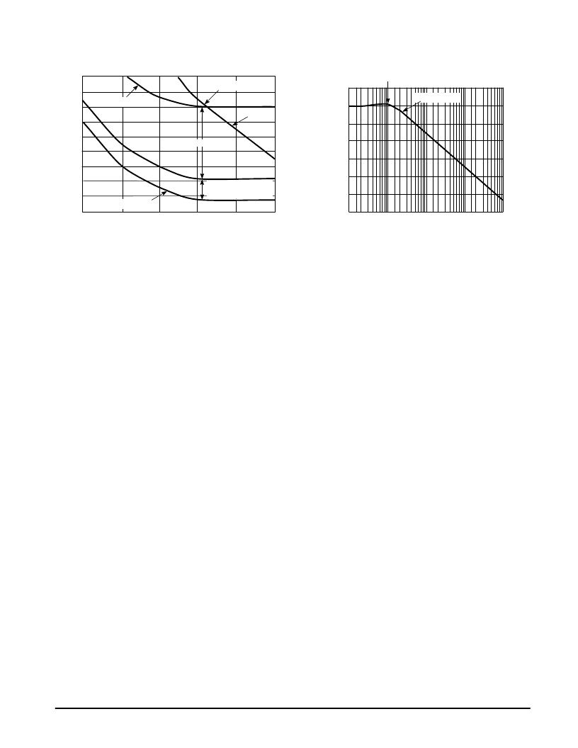
Figure 30. Graphical Analysis of
Optimum Bandwidth
–60
–70
–80
–90
–100
–110
–120
–130
–140
–150
d
10
100
1 k
10 k
100 k
1M
Hz
VCO
Optimum Bandwidth
Closed Loop Response
20 x log (Nt)
Crystal Reference
15 dB NF of the Noise
Contribution from Loop
Natural Frequency
Figure 31. Closed Loop Frequency Response
for
ζ
= 1
1.0 k
10
0
10
Hz
–20
–30
–40
–50
–60
0.1
100
1.0
–10
d
3 dB Bandwidth
In summary, follow the steps given below:
Step 1: Plot the phase noise of crystal reference and the
VCO on the same graph.
Step 2: Increase the phase noise of the crystal reference by
the noise contribution of the loop.
Step 3: Convert the divide–by–N to dB (20log 8 x N) and
increase the phase noise of the crystal reference by
that amount.
Step 4: The point at which the VCO phase noise crosses the
amplified phase noise of the crystal reference is the
point of the optimum loop bandwidth. This is
approximately 15 kHz in Figure 30.
Step 5: Correlate this loop bandwidth to the loop natural
frequency per Figure 31. In this case the 3.0 dB
bandwidth for a damping coefficient of 1 is 2.5 times
the loop’s natural frequency. The relationship
between the 3.0 dB loop bandwidth and the loop’s
“natural” frequency will vary for different values of
ζ
.
Making use of the equations defined in Figure 32, a
math tool or spread sheet is useful to select the
values for Ro and Co.
Appendix: Derivation of Loop Filter Transfer Function
The purpose of the loop filter is to convert the current from
the phase detector to a tuning voltage for the VCO. The total
transfer function is derived in two steps.
Step 1 is to find the voltage generated by the impedance of
the loop filter.
Step 2 is to find the transfer function from the input of the
loop filter to its output. The “voltage” times the “transfer
function” is the overall transfer function of the loop filter. To
use these equations in determining the overall transfer
function of a PLL, multiply the filter’s impedance by the gain
constant of the phase detector, then multiply that by the
filter’s transfer function. Figure 33 contains the transfer
function equations for the second, third, and fourth order PLL
filters.
PSpice Simulation
The use of PSpice or similar circuit simulation programs
can significantly reduce laboratory time when refining a PLL
design. The following describes the use of behavioral
modeling to develop useful models for studying loop filter
performance. In many applications the levels of sideband
spurs can also be studied.
Behavioral modeling is chosen, as opposed to discrete
device modeling, to improve performance and reduce
simulation time. PLL devices can contain several thousand
individual transistors. To simulate at this level can result in
generation of an enormous amount of data when compared
to a simpler behavioral model. For example, a logic NAND
gate can contain several transistors. Each of these requires a
data set for each of the transistor terminals. If a half dozen
transistors are used in the gate design, both current and
voltage measurements for each terminal of each device for
every node in the circuit is calculated. The gate can be
expressed as a behavioral model, which is treated and
simulated as a single device. Since PSpice sees this as a
single rather than multiple devices, the amount of
accumulated data is much less, resulting in a faster
simulation.
For applications using integrated circuits such as PLLs, it
is desirable to investigate the performance of the circuitry
added externally to the integrated circuit. By using behavioral
modeling rather than discrete device modeling to represent
the integrated circuit, the engineer is able to study the
performance of the design without the overhead contributed
by simulating the integrated circuit.
Phase Frequency Detector Model
The model for the phase frequency detector is derived
using the waveforms shown in Figure 20. Two signals are
present at the input of the phase frequency detector. These
are the reference input and the feedback from the VCO
and/or prescaler. The two signals are compared to determine
the lag/lead relationship between the two signals and pulses
generated to represent the leading edge of each signal. A
pulse whose width equals the lead of one input signal over
the other is generated by an RS flip–flop (RSFF). One RSFF
generates a pulse whose width equals the lead of the
reference signal over the feedback signal, and a second
RSFF generates a signal whose width is the lead of the
feedback signal over the reference signal. The logical model
for the phase frequency detector is shown in Figure 34.
相關(guān)PDF資料 |
PDF描述 |
|---|---|
| MC145230 | Dual PLL Frequency Synthesizers With DACs and Voltage Multipliers(帶DACs和電壓乘法器的雙PLL頻率合成器) |
| MC14528BCL | Dual Monostable Multivibrator |
| MC14528 | DEFLECTION PROCESSOR FOR MULTISYNC MONITORS |
| MC14528 | Dual Monostable Multivibrator |
| MC14528BFEL | Dual Monostable Multivibrator |
相關(guān)代理商/技術(shù)參數(shù) |
參數(shù)描述 |
|---|---|
| MC14522BCP | 制造商:Motorola Inc 功能描述:Counter, Down, Decade, 16 Pin, Plastic, DIP |
| MC14522BDW | 制造商:Motorola Inc 功能描述: |
| MC14526B AC7 WAF | 制造商:ON Semiconductor 功能描述: |
| MC14526BAC7 WAF | 制造商:ON Semiconductor 功能描述: |
| MC14526BCL | 制造商: 功能描述: 制造商:undefined 功能描述: |
發(fā)布緊急采購(gòu),3分鐘左右您將得到回復(fù)。