- 您現(xiàn)在的位置:買賣IC網(wǎng) > PDF目錄69009 > M30222FGGP 16-BIT, FLASH, MICROCONTROLLER, PQFP100 PDF資料下載
參數(shù)資料
| 型號: | M30222FGGP |
| 元件分類: | 微控制器/微處理器 |
| 英文描述: | 16-BIT, FLASH, MICROCONTROLLER, PQFP100 |
| 封裝: | PLASTIC, QFP-100 |
| 文件頁數(shù): | 51/236頁 |
| 文件大?。?/td> | 1955K |
| 代理商: | M30222FGGP |
第1頁第2頁第3頁第4頁第5頁第6頁第7頁第8頁第9頁第10頁第11頁第12頁第13頁第14頁第15頁第16頁第17頁第18頁第19頁第20頁第21頁第22頁第23頁第24頁第25頁第26頁第27頁第28頁第29頁第30頁第31頁第32頁第33頁第34頁第35頁第36頁第37頁第38頁第39頁第40頁第41頁第42頁第43頁第44頁第45頁第46頁第47頁第48頁第49頁第50頁當(dāng)前第51頁第52頁第53頁第54頁第55頁第56頁第57頁第58頁第59頁第60頁第61頁第62頁第63頁第64頁第65頁第66頁第67頁第68頁第69頁第70頁第71頁第72頁第73頁第74頁第75頁第76頁第77頁第78頁第79頁第80頁第81頁第82頁第83頁第84頁第85頁第86頁第87頁第88頁第89頁第90頁第91頁第92頁第93頁第94頁第95頁第96頁第97頁第98頁第99頁第100頁第101頁第102頁第103頁第104頁第105頁第106頁第107頁第108頁第109頁第110頁第111頁第112頁第113頁第114頁第115頁第116頁第117頁第118頁第119頁第120頁第121頁第122頁第123頁第124頁第125頁第126頁第127頁第128頁第129頁第130頁第131頁第132頁第133頁第134頁第135頁第136頁第137頁第138頁第139頁第140頁第141頁第142頁第143頁第144頁第145頁第146頁第147頁第148頁第149頁第150頁第151頁第152頁第153頁第154頁第155頁第156頁第157頁第158頁第159頁第160頁第161頁第162頁第163頁第164頁第165頁第166頁第167頁第168頁第169頁第170頁第171頁第172頁第173頁第174頁第175頁第176頁第177頁第178頁第179頁第180頁第181頁第182頁第183頁第184頁第185頁第186頁第187頁第188頁第189頁第190頁第191頁第192頁第193頁第194頁第195頁第196頁第197頁第198頁第199頁第200頁第201頁第202頁第203頁第204頁第205頁第206頁第207頁第208頁第209頁第210頁第211頁第212頁第213頁第214頁第215頁第216頁第217頁第218頁第219頁第220頁第221頁第222頁第223頁第224頁第225頁第226頁第227頁第228頁第229頁第230頁第231頁第232頁第233頁第234頁第235頁第236頁
1-145
Under
development
Specifications in this manual are tentative and subject to change
Rev. H
Serial I/O (3, 4)
MITSUBISHI MICROCOMPUTERS
M30222 Group
SINGLE-CHIP 16-BIT CMOS MICROCOMPUTER
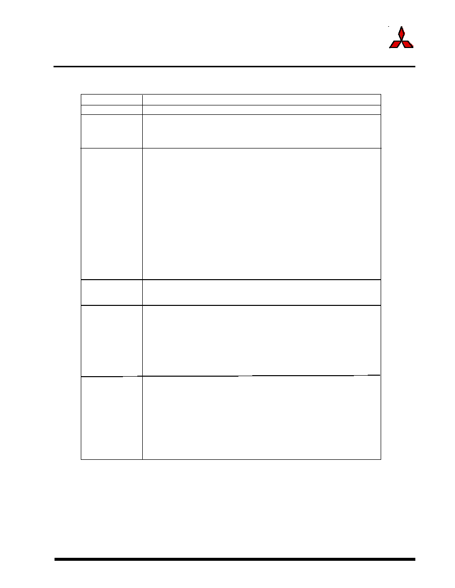
Table 1.44. Specifications of S I/O 3, 4
Note 1: n is a value from 00 16 through FF 16 set in the S I/Oi transfer rate register (i = 3, 4).
Note 2: With the external clock selected:
Before data can be written to the SI/Oi transmit/receive register (addresses 036016, 036416), the
CLKi pin input must be in the low state. Also, before rewriting the SI/Oi Control Register (addresses
036216, 036616)’s bit 7 (SOUTi initial value set bit), make sure the CLKi pin input is held low.
The S I/Oi circuit keeps on with the shift operation as long as the synchronous clock is entered in it.
Note 3: If the internal clock is used for the synchronous clock, the transfer clock signal output, when enabled,
Item
Transfer data format
Transfer clock
Conditions for
Interrupt request
generation timing
Select function
Precaution
Specifications
Transfer data length: 8 bits
With the internal clock selected (bit 6 of 036216, 036616 = “1”): f1/2(ni+1),
f8/2(ni+1), f32/2(ni+1) (Note 1)
To start transmission/reception, the following requirements must be met:
- Select the synchronous clock (use bit 6 of 036216, 036616).
Select a frequency dividing ratio if the internal clock has been selected (use bits
0 and 1 of 036216 , 036616).
- SOUTi initial value set bit (use bit 7 of 036216, 036616)= 1.
- S I/Oi port select bit (bit 3 of 036216, 036616) = 1.
- Select the transfer direction (use bit 5 of 036216, 036616)
-Write transfer data to SI/Oi transmit/receive register (0360 16, 036416 )
To use S I/Oi interrupts, the following requirements must be met:
- Clear the SI/Oi interrupt request bit before writing transfer data to the SI/Oi
transmit/receive register (bit 3 of 004916 , 004816) = 0.
Rising edge of the last transfer clock. (Note 3)
LSB first or MSB first selection
Whether transmission/reception begins with bit 0 (LSB) or bit 7 (MSB) can be
selected.
Function for setting an SOUTi initial value selection
When using an external clock for the transfer clock, the user can choose the
SOUTi pin output level during a non-transfer time. For details on how to set, see
Figure 1.112.
Unlike UART0–2, SI/Oi (i = 3, 4) is not divided for transfer register and buffer.
Therefore, do not write the next transfer data to the SI/Oi transmit/receive register
(addresses 036016, 036416) during a transfer. When the internal clock is selected
for the transfer clock, SOUTi holds the last data for a 1/2 transfer clock period after
it finished transferring and then goes to a high-impedance state. However, if the
transfer data is written to the SI/Oi transmit/receive register (addresses 036016 ,
036416) during this time, SOUTi is placed in the high-impedance state immediately
upon writing and the data hold time is thereby reduced.
i
If an internal clock is selected, set the bit rate generator divisor (036316, 036716)
[It is not necessry to start transmit/receive. It is only needed for operation as
intended]
stops at the "H" state after transmission is completed.
With the external clock selected (bit 6 of 036216, 036616 = 0):
Input from the CLKi terminal (Note 2)
Therefore, stop the synchronous clock immediately when count reaches eight. If selected, the internal
clock stops automatically clocking the SIO channel.
transmit/receive
start
相關(guān)PDF資料 |
PDF描述 |
|---|---|
| M30222FGFP | 16-BIT, FLASH, MICROCONTROLLER, PQFP100 |
| M30240M6-XXXFP | 16-BIT, MROM, 12 MHz, MICROCONTROLLER, PQFP80 |
| M30240M6-XXXFP | 16-BIT, MROM, 12 MHz, MICROCONTROLLER, PQFP80 |
| M30240M5-XXXFP | 16-BIT, MROM, 12 MHz, MICROCONTROLLER, PQFP80 |
| M30240M6-XXXXFP | 16-BIT, MROM, 12 MHz, MICROCONTROLLER, PQFP80 |
相關(guān)代理商/技術(shù)參數(shù) |
參數(shù)描述 |
|---|---|
| M30222FG-XXXFP | 制造商:MITSUBISHI 制造商全稱:Mitsubishi Electric Semiconductor 功能描述:SINGLE-CHIP 16-BIT CMOS MICROCOMPUTER |
| M30222FG-XXXGP | 制造商:MITSUBISHI 制造商全稱:Mitsubishi Electric Semiconductor 功能描述:SINGLE-CHIP 16-BIT CMOS MICROCOMPUTER |
| M3024 | 功能描述:速度傳感器 ELECTRO RoHS:否 制造商:Honeywell 最大工作溫度:+ 120 C 電源電壓: 電源電流: 輸出電壓:190 V 工作電源電壓: 安裝風(fēng)格:Screw 最小工作溫度:- 55 C 系列:High Output VRS |
| M30240 | 制造商:MITSUBISHI 制造商全稱:Mitsubishi Electric Semiconductor 功能描述:M30240 Group Specification |
| M30240E1 | 制造商:MITSUBISHI 制造商全稱:Mitsubishi Electric Semiconductor 功能描述:SINGLE-CHIP 16-BIT CMOS MICROCOMPUTER |
發(fā)布緊急采購,3分鐘左右您將得到回復(fù)。