- 您現(xiàn)在的位置:買賣IC網 > PDF目錄69009 > M30222FGGP 16-BIT, FLASH, MICROCONTROLLER, PQFP100 PDF資料下載
參數資料
| 型號: | M30222FGGP |
| 元件分類: | 微控制器/微處理器 |
| 英文描述: | 16-BIT, FLASH, MICROCONTROLLER, PQFP100 |
| 封裝: | PLASTIC, QFP-100 |
| 文件頁數: | 36/236頁 |
| 文件大小: | 1955K |
| 代理商: | M30222FGGP |
第1頁第2頁第3頁第4頁第5頁第6頁第7頁第8頁第9頁第10頁第11頁第12頁第13頁第14頁第15頁第16頁第17頁第18頁第19頁第20頁第21頁第22頁第23頁第24頁第25頁第26頁第27頁第28頁第29頁第30頁第31頁第32頁第33頁第34頁第35頁當前第36頁第37頁第38頁第39頁第40頁第41頁第42頁第43頁第44頁第45頁第46頁第47頁第48頁第49頁第50頁第51頁第52頁第53頁第54頁第55頁第56頁第57頁第58頁第59頁第60頁第61頁第62頁第63頁第64頁第65頁第66頁第67頁第68頁第69頁第70頁第71頁第72頁第73頁第74頁第75頁第76頁第77頁第78頁第79頁第80頁第81頁第82頁第83頁第84頁第85頁第86頁第87頁第88頁第89頁第90頁第91頁第92頁第93頁第94頁第95頁第96頁第97頁第98頁第99頁第100頁第101頁第102頁第103頁第104頁第105頁第106頁第107頁第108頁第109頁第110頁第111頁第112頁第113頁第114頁第115頁第116頁第117頁第118頁第119頁第120頁第121頁第122頁第123頁第124頁第125頁第126頁第127頁第128頁第129頁第130頁第131頁第132頁第133頁第134頁第135頁第136頁第137頁第138頁第139頁第140頁第141頁第142頁第143頁第144頁第145頁第146頁第147頁第148頁第149頁第150頁第151頁第152頁第153頁第154頁第155頁第156頁第157頁第158頁第159頁第160頁第161頁第162頁第163頁第164頁第165頁第166頁第167頁第168頁第169頁第170頁第171頁第172頁第173頁第174頁第175頁第176頁第177頁第178頁第179頁第180頁第181頁第182頁第183頁第184頁第185頁第186頁第187頁第188頁第189頁第190頁第191頁第192頁第193頁第194頁第195頁第196頁第197頁第198頁第199頁第200頁第201頁第202頁第203頁第204頁第205頁第206頁第207頁第208頁第209頁第210頁第211頁第212頁第213頁第214頁第215頁第216頁第217頁第218頁第219頁第220頁第221頁第222頁第223頁第224頁第225頁第226頁第227頁第228頁第229頁第230頁第231頁第232頁第233頁第234頁第235頁第236頁
1-131
Under
development
Specifications in this manual are tentative and subject to change
Rev. H
UART2 in I2C Mode
MITSUBISHI MICROCOMPUTERS
M30222 Group
SINGLE-CHIP 16-BIT CMOS MICROCOMPUTER
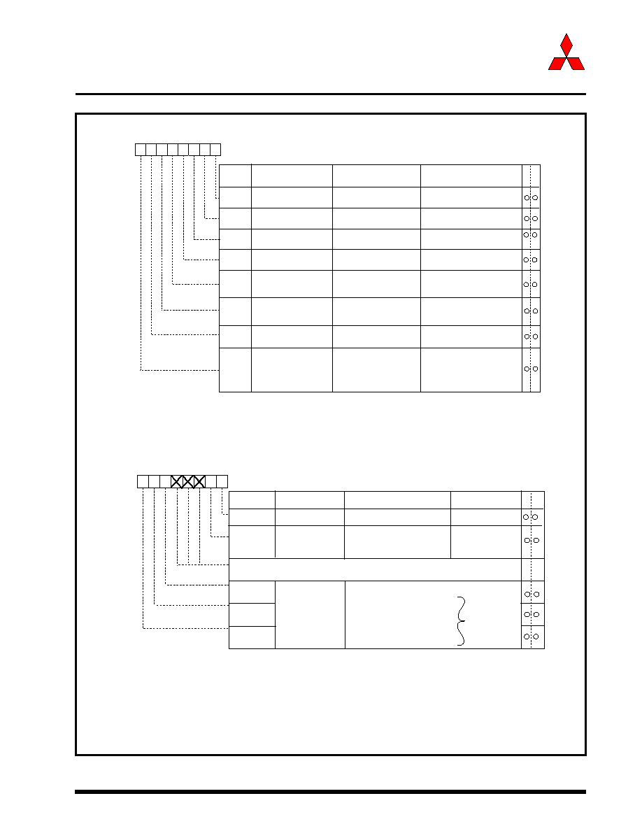
Fig. 1.104. UART2 special mode register
Symbol
Address
When reset
U2SMR3
037516
0016
UART2 Special mode register 3 (I2C and SPI bus exclusive use register)
DL0
DL1
DL2
0 : Normal mode
1 : SPI mode
Bit name
Bit symbol
b7
b6
b5
b4
b3
b2
b1
b0
SPIM
CPHA
SPI mode select bit
0 0 0 : Analog delay is selected
0 0 1 : 2 cycle of 1/f(X IN)
0 1 0 : 3 cycle of 1/f(X IN)
0 1 1 : 4 cycle of 1/f(X IN)
1 0 0 : 5 cycle of 1/f(X IN)
1 0 1 : 6 cycle of 1/f(X IN)
1 1 0 : 7 cycle of 1/f(X IN)
1 1 1 : 8 cycle of 1/f(X IN)
b7 b6 b5
W
R
SPI clock-phase
select bit
Function during clock
synchronous serial I/O mode
Function during
UART mode
0 : Data latched on
falling clock edge
1 : Data latched on
rising clock edge
Must always be "0'
Digital delay
is selected
SDA digital delay
set up bit (Note
1, 2, 3, 4, 5)
Nothing is assigned. In an attempt to write to these bits, write "0". When read the
value is indeterminate. However, when SDDS = "1", a "0" value is read.
_ _
Note 1:
This bit can be read or written to when UART2 special mode register U2SMR at address 037716 bit 7
(SDDS: SDA digital delay select bit) = "1". When the initial value of UART2 special mode register 3
(U2SMR3 is read after setting SDDS = "1", the value is "0016". When writing to U2SMR3 after setting
SDDS = "1", be sure to write 0s to bits 0 - 4. When SDDS = "0", This register cannot be written to;
when read, the value is indeterminate.
Note 2:
These bits are initialized to "000" when SDDS = "0", with the analog delay circuit selected. After a reset
these bits are set to "000", with the analog delay circuit selected. However, because these bits can be read
only when SDDS = "1", the value read from these bits when SDDS = "0" is indeterminate.
Note 3:
When analog delay is selected, only the analog delay value is effective; when digital delay is selected,
only the digital delay value is effective.
Note 4:
The amount of delay varies with the load on SCL and SDA pins. Also, when using an external clock,
the amount of delay increases by about 100ns. Be sure to take this into account when using this device.
Note 5:
Reset values for SPIM and CPHA are not affected by the state of SDDs. Their reset values are always "0".
(Note 1)
UART2 Special mode register
Symbol
Address
When reset
U2SMR
037716
0016
b7
b6
b5
b4
b3
b2
b1
b0
Bit name
Bit
symbol
W
R
Function
(During UART mode)
Function
(During clock synchronous
serial I/O mode)
ABSCS
ACSE
SSS
IIC mode selection bit
Bus busy flag
0 : STOP condition detected
1 : START condition detected
SCLL sync output
enable bit
Bus collision detect
sampling
clock select bit
Arbitration lost detecting
flag control bit
0 : Normal mode
1 : IIC mode
0 : Update per bit
1 : Update per byte
IICM
ABC
BBS
LSYN
0 : Ordinary
1 : Falling edge of RxD2
0 : Disabled
1 : Enabled
Transmit start condition
select bit
Must always be “0”
0 : Rising edge of transfer
clock
1 : Underflow signal of timer A0
Auto clear function
select bit of transmit
enable bit
0 : No auto clear function
1 : Auto clear at occurrence of
bus collision
Must always be “0”
Note 1: Nothing but "0" may be written.
Note 2: When not in I 2C mode, do not set this bit by writing a "1". During normal mode, fix it to "0". When this
(Note 1)
SDDS
SDA digital delay select
bit (Note 2, 3)
0 : Analog delay output is
selected
1 : Digital delay output is
selected (Must always
be "0" when not using
I2C mode)
Must always be "0"
bit - "0" , UART2 special mode register 3 (U2SMR3 at address 037516) bits 7 to 5 (DL2 to DL0 = SDA
digital delay setup bits) are initialized to "000", with the analog delay circuit selected. Also, when SDDS
= "0", the U2SMR3 register cannot be read or written to.
Note 3: When analog delay is selected, only the analog delay value is effective; when digital delay is selected
only the digital delay value is effective.
相關PDF資料 |
PDF描述 |
|---|---|
| M30222FGFP | 16-BIT, FLASH, MICROCONTROLLER, PQFP100 |
| M30240M6-XXXFP | 16-BIT, MROM, 12 MHz, MICROCONTROLLER, PQFP80 |
| M30240M6-XXXFP | 16-BIT, MROM, 12 MHz, MICROCONTROLLER, PQFP80 |
| M30240M5-XXXFP | 16-BIT, MROM, 12 MHz, MICROCONTROLLER, PQFP80 |
| M30240M6-XXXXFP | 16-BIT, MROM, 12 MHz, MICROCONTROLLER, PQFP80 |
相關代理商/技術參數 |
參數描述 |
|---|---|
| M30222FG-XXXFP | 制造商:MITSUBISHI 制造商全稱:Mitsubishi Electric Semiconductor 功能描述:SINGLE-CHIP 16-BIT CMOS MICROCOMPUTER |
| M30222FG-XXXGP | 制造商:MITSUBISHI 制造商全稱:Mitsubishi Electric Semiconductor 功能描述:SINGLE-CHIP 16-BIT CMOS MICROCOMPUTER |
| M3024 | 功能描述:速度傳感器 ELECTRO RoHS:否 制造商:Honeywell 最大工作溫度:+ 120 C 電源電壓: 電源電流: 輸出電壓:190 V 工作電源電壓: 安裝風格:Screw 最小工作溫度:- 55 C 系列:High Output VRS |
| M30240 | 制造商:MITSUBISHI 制造商全稱:Mitsubishi Electric Semiconductor 功能描述:M30240 Group Specification |
| M30240E1 | 制造商:MITSUBISHI 制造商全稱:Mitsubishi Electric Semiconductor 功能描述:SINGLE-CHIP 16-BIT CMOS MICROCOMPUTER |
發(fā)布緊急采購,3分鐘左右您將得到回復。