- 您現(xiàn)在的位置:買賣IC網(wǎng) > PDF目錄369885 > LXT350PE PCM TRANSCEIVER|SINGLE|CEPT PCM-30/E-1|CMOS|LDCC|28PIN|PLASTIC PDF資料下載
參數(shù)資料
| 型號: | LXT350PE |
| 英文描述: | PCM TRANSCEIVER|SINGLE|CEPT PCM-30/E-1|CMOS|LDCC|28PIN|PLASTIC |
| 中文描述: | 的PCM收發(fā)器|單|優(yōu)稅PCM-30/E-1 |的CMOS | LDCC | 28腳|塑料 |
| 文件頁數(shù): | 39/50頁 |
| 文件大小: | 1197K |
| 代理商: | LXT350PE |
第1頁第2頁第3頁第4頁第5頁第6頁第7頁第8頁第9頁第10頁第11頁第12頁第13頁第14頁第15頁第16頁第17頁第18頁第19頁第20頁第21頁第22頁第23頁第24頁第25頁第26頁第27頁第28頁第29頁第30頁第31頁第32頁第33頁第34頁第35頁第36頁第37頁第38頁當前第39頁第40頁第41頁第42頁第43頁第44頁第45頁第46頁第47頁第48頁第49頁第50頁
T1/E1 Short Haul Transceiver with Crystal-less Jitter Attenuation
—
LXT350
Datasheet
39
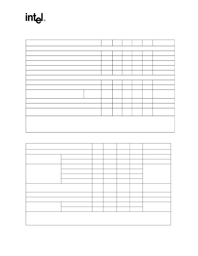
Table 24. DC Electrical Characteristics
Parameter
Sym
Min
Typ
Max
Unit
Test Conditions
Digital I/O pins
High level input voltage
1,2
(pins 1-4, 23-25)
4
V
IH
2.0
–
–
V
Low level input voltage
1,2
(pins 1-4, 23-25)
4
V
IL
–
–
0.8
V
High level output voltage
1,2
(pins 6-8, 12, 23, 25)
4
V
OH
2.4
–
–
V
I
OUT
= -400
μ
A
Low level output voltage
1,2
(pins 6-8, 12, 23, 25)
4
V
OL
–
–
0.4
V
I
OUT
= 1.6 mA
Tri-state leakage current
1
(all outputs)
I
3
L
0
–
±10
μ
A
Mode input pins
High level input voltage
3
(pins 5, 9, 11, 26-28)
4
V
IH
3.5
–
–
V
Midrange output voltage
3
(pins 5, 9, 11, 26-28)
4
V
OM
2.3
–
2.7
V
Low level input voltage
3
(pins 5, 9, 11, 26-28)
4
Host Mode
H/W Mode
V
IL
V
IL
–
–
–
–
0.8
1.5
V
V
Input leakage current (pins 5, 9, 11, 26-28)
4
I
LL
0
–
±50
μ
A
Tri-state leakage current
1
(all outputs)
I3L
0
–
±10
μ
A
TTIP/TRING leakage current
I
TR
–
–
1.2
mA
In power down
and tristate
1. Functionality of pin 23 and 25 depends on mode. See Host mode and Hardware mode description.
2. Output drivers will output CMOS logic levels into CMOS loads.
3. As an alternative to supplying 2.3 - 2.7 V to these pins, they may be left open.
4. Listed pins are for the PLCC package. Refer to
“
Pin Assignments and Signal Descriptions
”
on page 8
for the 44-pin QFP
package.
Table 25. Analog Characteristics
Parameter
Min
Typ
1
Max
Unit
Test Conditions
Recommended output load on TTIP/TRING
50
–
200
AMI output pulse amplitudes
T1
2.4
3.0
3.6
V
R
L
= 100
E1
2.7
3.0
3.3
V
R
L
= 120
Jitter added by the
transmitter
2
10 Hz - 8 kHz
3
–
–
0.02
UI
8 kHz - 40 kHz
3
–
–
0.025
UI
10 Hz - 40 kHz
3
–
–
0.025
UI
Broad Band
–
–
0.05
UI
Receiver sensitivity
0
–
18
dB
@ 1024 kHz
1.431
Allowable consecutive zeros before LOS (T1)
160
175
190
–
Allowable consecutive zeros before LOS (E1)
–
32
–
–
Input jitter tolerance (T1)
10 kHz - 100 kHz
0.4
–
–
UI
0 dB line
AT&T Pub 62411
1 Hz
3
138
–
–
UI
1. Typical figures are at 25
°
C and are for design aid only; not guaranteed and not subject to production testing.
2. Input signal to TCLK is jitter-free. The Jitter Attenuator is in the receive path or disabled.
3. Guaranteed by characterization; not subject to production testing.
4. Circuit attenuates jitter at 20 dB/decade above the corner frequency.
相關(guān)PDF資料 |
PDF描述 |
|---|---|
| LXT361LE | Telecommunication IC |
| LXT361PE | Telecommunication IC |
| LXT362LE | PCM TRANSCEIVER|SINGLE|T-1(DS1)|CMOS|QFP|44PIN|PLASTIC |
| LXT362PE | PCM TRANSCEIVER|SINGLE|T-1(DS1)|CMOS|LDCC|28PIN|PLASTIC |
| LXT362QE | PCM TRANSCEIVER|SINGLE|T-1(DS1)|CMOS|QFP|44PIN|PLASTIC |
相關(guān)代理商/技術(shù)參數(shù) |
參數(shù)描述 |
|---|---|
| LXT350QE | 制造商:LEVEL1 功能描述: |
| LXT351 | 制造商:INTEL 制造商全稱:Intel Corporation 功能描述:T1/E1 Short Haul Transceiver with Crystal-less Jitter Attenuation |
| LXT351PE | 制造商:INTEL 制造商全稱:Intel Corporation 功能描述:PCM TRANSCEIVER|SINGLE|CEPT PCM-30/E-1|CMOS|LDCC|28PIN|PLASTIC |
| LXT351QE | 制造商:INTEL 制造商全稱:Intel Corporation 功能描述:PCM TRANSCEIVER|SINGLE|CEPT PCM-30/E-1|CMOS|QFP|44PIN|PLASTIC |
| LXT360 | 制造商:LVL1 制造商全稱:LVL1 功能描述:Integrated T1/E1 LH/SH Transceivers for DS1/DSX-1/CSU or NTU/ISDN PRI Applications |
發(fā)布緊急采購,3分鐘左右您將得到回復。