- 您現(xiàn)在的位置:買賣IC網(wǎng) > PDF目錄379205 > IBM13Q8739CC (IBM Microeletronics) 8M x 72 Registered SDRAM Module(帶寄存同步動態(tài)RAM模塊(8M x 72高速存儲器陣列結(jié)構(gòu))) PDF資料下載
參數(shù)資料
| 型號: | IBM13Q8739CC |
| 廠商: | IBM Microeletronics |
| 英文描述: | 8M x 72 Registered SDRAM Module(帶寄存同步動態(tài)RAM模塊(8M x 72高速存儲器陣列結(jié)構(gòu))) |
| 中文描述: | 8米× 72注冊內(nèi)存模塊(帶寄存同步動態(tài)內(nèi)存模塊(8米× 72高速存儲器陣列結(jié)構(gòu))) |
| 文件頁數(shù): | 15/56頁 |
| 文件大小: | 903K |
| 代理商: | IBM13Q8739CC |
第1頁第2頁第3頁第4頁第5頁第6頁第7頁第8頁第9頁第10頁第11頁第12頁第13頁第14頁當(dāng)前第15頁第16頁第17頁第18頁第19頁第20頁第21頁第22頁第23頁第24頁第25頁第26頁第27頁第28頁第29頁第30頁第31頁第32頁第33頁第34頁第35頁第36頁第37頁第38頁第39頁第40頁第41頁第42頁第43頁第44頁第45頁第46頁第47頁第48頁第49頁第50頁第51頁第52頁第53頁第54頁第55頁第56頁
IBM13Q8739CC
8M x 72 Registered SDRAM Module
08J0513.E24526
Revised 4/98
IBM Corporation. All rights reserved.
Use is further subject to the provisions at the end of this document.
Page 15 of 56
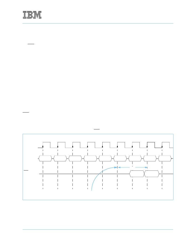
Auto-Precharge Operation
Before a new row in an active bank can be opened, the active bank must be precharged using either the Pre-
charge command or the auto-precharge function. When a Read or a Write command is given to the DIMM,
the CAS timing accepts one extra address, column address A10/AP, to allow the active bank to automatically
begin precharge at the earliest possible moment during the Burst Read or Write cycle. If A10/AP is low when
the READ or WRITE command is issued, then normal Read or Write Burst operation is executed and the
bank remains active at the completion of the burst sequence. If A10/AP is high when the Read or Write com-
mand is issued, then the auto-precharge function is engaged.
During autoprecharge, a Read command will execute normally, except the active bank will begin to precharge
before all Burst Read cycles have been completed. This feature allows the Precharge operation to be partially
or completely hidden during the Burst Read cycles (dependent upon burst length), improving system perfor-
mance for random data access. Auto-precharge can also be implemented during Write commands although
precharge cannot begin any sooner than is possible by issuing the Precharge command directly to the
device.
A Read or Write command without auto-precharge can be terminated in the midst of a Burst operation. How-
ever, a Read or Write command with auto-precharge cannot be interrupted before the entire Burst operation
is completed. Therefore use of a Read, Write, Precharge, or Burst Stop command is prohibited during a Read
or Write cycle with auto-precharge.
If A10/AP is high when a Read command is issued, the Read with Auto-Precharge function is initiated. The
SDRAM automatically enters the Precharge operation two clocks after the Read command is registered for
CAS latencies of 2. Once the Precharge operation has started the bank cannot be reactivated until the Pre-
charge time (t
RP
) has been satisfied. Note that the device will not respond to the Auto-Precharge command if
the device is programmed for full page Burst Read or Write cycles, or full page Burst Read cycles with single
Write operation.
If A10/AP is high when a Write command is issued, the Write with Auto-Precharge function is initiated. The
SDRAM automatically enters the Precharge operation one clock delay from the last Burst Write cycle. This
delay is referred to as t
DPL
. The bank undergoing auto-precharge cannot be reactivated until t
DPL
and t
RP
are
satisfied. This is referred to as t
DAL,
Data-in to Active delay (t
DAL
= t
DPL
+ t
RP
).
Burst Read with Autoprecharge
(Burst Length = 2, CAS latency = 2)
COMMAND
NOP
NOP
NOP
NOP
Auto-Precharge
CK0
T0
T2
T1
T3
T4
T5
T6
T7
T8
NOP
BANK A
ACTIVE
NOP
NOP
t
RP
t
CK2,
DQs
CAS latency = 2
Begin Autoprecharge
Bank can be reactivated at completion of tRP
DOUT A0
DOUT A1
Note: Data is delayed one cycle due to on-DIMM pipeline register
*
相關(guān)PDF資料 |
PDF描述 |
|---|---|
| IBM13T16644NPA | 16M x 64 PC100 SDRAM(1MB PC100 同步動態(tài)RAM) |
| IBM13T2649JC | 2M x 64 SDRAM SO DIMM(Small Outline Dual In-Line Memory Module)(2M x 64 小外形雙列直插同步動態(tài)RAM模塊) |
| IBM13T2649NC | 2M x 64 SDRAM SO DIMM(2M x 64小外形雙列直插同步動態(tài)RAM模塊) |
| IBM13T4644MC | 1M x 64 SDRAM SO DIMM(1M x 64 同步動態(tài)RAM模塊) |
| IBM13T1649NC | 1M x 64 SDRAM SO DIMM(1M x 64 同步動態(tài)RAM模塊) |
相關(guān)代理商/技術(shù)參數(shù) |
參數(shù)描述 |
|---|---|
| IBM14H5481 | 制造商:AVED Memory Products 功能描述: |
| IBM14H5540 | 制造商:AVED MEMORY PRODUCTS 功能描述: 制造商:AVED Memory Products 功能描述: |
| IBM17R8251 | 制造商:AVED Memory Products 功能描述: |
| IBM17R8252 | 制造商:AVED Memory Products 功能描述: |
| IBM1805T | 制造商:Schneider Electric 功能描述:IBM1805T |
發(fā)布緊急采購,3分鐘左右您將得到回復(fù)。