- 您現(xiàn)在的位置:買賣IC網(wǎng) > PDF目錄382861 > AX88796 (Electronic Theatre Controls, Inc.) 3-in-1 Local Bus Fast Ethernet Controller PDF資料下載
參數(shù)資料
| 型號(hào): | AX88796 |
| 廠商: | Electronic Theatre Controls, Inc. |
| 英文描述: | 3-in-1 Local Bus Fast Ethernet Controller |
| 中文描述: | 3合1本地總線快速以太網(wǎng)控制器 |
| 文件頁數(shù): | 14/71頁 |
| 文件大小: | 931K |
| 代理商: | AX88796 |
第1頁第2頁第3頁第4頁第5頁第6頁第7頁第8頁第9頁第10頁第11頁第12頁第13頁當(dāng)前第14頁第15頁第16頁第17頁第18頁第19頁第20頁第21頁第22頁第23頁第24頁第25頁第26頁第27頁第28頁第29頁第30頁第31頁第32頁第33頁第34頁第35頁第36頁第37頁第38頁第39頁第40頁第41頁第42頁第43頁第44頁第45頁第46頁第47頁第48頁第49頁第50頁第51頁第52頁第53頁第54頁第55頁第56頁第57頁第58頁第59頁第60頁第61頁第62頁第63頁第64頁第65頁第66頁第67頁第68頁第69頁第70頁第71頁
ASIX ELECTRONICS CORPORATION
14
AX88796 L 3-in-1 Local Bus Fast Ethernet Controller
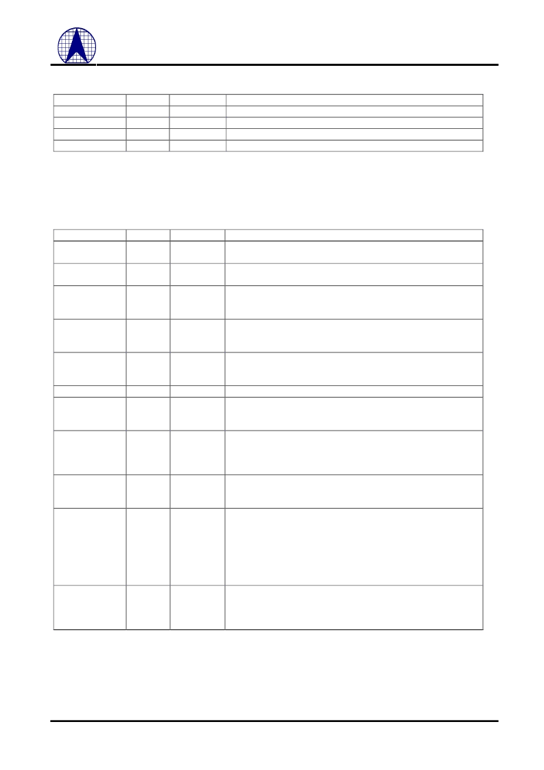
2.4 EEPROM Signals Group
SIGNAL
TYPE
PIN NO.
EECS
O
51
EEPROM Chip Select : EEPROM chip select signal.
EECK
O/PD
50
EEPROM Clock : Signal connected to EEPROM clock pin.
EEDI
O
49
EEPROM Data In : Signal connected to EEPROM data input pin.
EEDO
I/PU
48
EEPROM Data Out : Signal connected to EEPROM data output pin.
DESCRIPTION
Tab - 4 EEPROM bus interface signals group
2.5 MII interface signals group(Optional)
SIGNAL
TYPE
PIN NO.
RXD[3:0]
CRS
I/PD
DESCRIPTION
I/PU
98 – 95
Receive Data : RXD[3:0] is driven by the PHY synchronously with
respect to RX_CLK.
Carrier Sense : Asynchronous signal CRS is asserted by the PHY
when either the transmit or receive medium is non-idle.
Receive Data Valid : RX_DV is driven by the PHY synchronously
with respect to RX_CLK. Asserted high when valid data is present on
RXD [3:0].
No Support Receive Error : RX_ER ,is driven by PHY and synchronous to
RX_CLK, is asserted for one or more RX_CLK periods to indicate to
the port that an error has detected.
99
Receive Clock : RX_CLK is a continuous clock that provides the
timing reference for the transfer of the RX_DV,RXD[3:0] and
RX_ER signals from the PHY to the MII port of the repeater.
101
Collision : this signal is driven by PHY when collision is detected.
108
Transmit Enable : TX_EN is transition synchronously with respect to
the rising edge of TX_CLK. TX_EN indicates that the port is
presenting nibbles on TXD [3:0] for transmission.
112 – 109 Transmit Data : TXD[3:0] is transition synchronously with respect to
the rising edge of TX_CLK. For each TX_CLK period in which
TX_EN is asserted, TXD[3:0] are accepted for transmission by the
PHY.
107
Transmit Clock : TX_CLK is a continuous clock from PHY. It
provides the timing reference for the transfer of the TX_EN and
TXD[3:0] signals from the MII port to the PHY.
67
Station Management Data Clock : The timing reference for MDIO.
All data transfers on MDIO are synchronized to the rising edge of this
clock. The signal output reflects MDC register value. About MDC
register, please refer to MII/EEPROM Management register bit 0.
MDC clock frequency is a 2.5MHz maximum accourding to IEEE
802.3u MII specification. Acturely, many PHYs are designed to accept
higher frequency than 2.5MHz.
66
Station Management Data Input/Output :Serial data input/output
transfers from/to the PHYs . The transfer protocol has to meet the
IEEE 802.3u MII specification. For more information, please refer to
section 6.5 CPU Access MII Station Management functions.
100
RX_DV
I/PD
102
RX_ER
(Omit)
RX_CLK
I/PU
COL
TX_EN
I/PD
O
TXD[3:0]
O
TX_CLK
I/PU
MDC
O/PU
MDIO
I/O/PU
Tab - 5 MII interface signals group
相關(guān)PDF資料 |
PDF描述 |
|---|---|
| AX88796L | 3-in-1 Local Bus Fast Ethernet Controller |
| AY3-8910 | PROGRAMMABLE SOUND GENERATOR |
| AY-3-8910 | PROGRAMMABLE SOUND GENERATOR |
| AY-3-8912 | PROGRAMMABLE SOUND GENERATOR |
| AY-3-8913 | PROGRAMMABLE SOUND GENERATOR |
相關(guān)代理商/技術(shù)參數(shù) |
參數(shù)描述 |
|---|---|
| AX88796ALF | 制造商:ASIX 功能描述:10/100 MAC,COMMERCIAL 128PIN |
| AX88796BLF | 制造商:Asix Electronics 功能描述:IEEE802.3 / IEEE802.3u LAN standard Ethernet 3.3V 64LQFP Tray 制造商:ASIX 功能描述:10/100 MAC,COMMERCIAL 64PIN |
| AX88796BLI | 制造商:未知廠家 制造商全稱:未知廠家 功能描述:High-Performance Non-PCI Single-Chip 8/16 bit 10/100M Fast Ethernet Controller |
| AX88796C | 制造商:ASIX 制造商全稱:ASIX 功能描述:Low-Power SPI or Non-PCI Ethernet Controller |
| AX88796CLF | 制造商:ASIX Electronics Corporation 功能描述: |
發(fā)布緊急采購,3分鐘左右您將得到回復(fù)。