- 您現(xiàn)在的位置:買賣IC網(wǎng) > PDF目錄156622 > 4565B2 ATM/SONET/SDH SUPPORT CIRCUIT, PBGA909 PDF資料下載
參數(shù)資料
| 型號(hào): | 4565B2 |
| 元件分類: | 數(shù)字傳輸電路 |
| 英文描述: | ATM/SONET/SDH SUPPORT CIRCUIT, PBGA909 |
| 封裝: | PLASTIC, BGA-909 |
| 文件頁(yè)數(shù): | 49/61頁(yè) |
| 文件大小: | 1691K |
| 代理商: | 4565B2 |
第1頁(yè)第2頁(yè)第3頁(yè)第4頁(yè)第5頁(yè)第6頁(yè)第7頁(yè)第8頁(yè)第9頁(yè)第10頁(yè)第11頁(yè)第12頁(yè)第13頁(yè)第14頁(yè)第15頁(yè)第16頁(yè)第17頁(yè)第18頁(yè)第19頁(yè)第20頁(yè)第21頁(yè)第22頁(yè)第23頁(yè)第24頁(yè)第25頁(yè)第26頁(yè)第27頁(yè)第28頁(yè)第29頁(yè)第30頁(yè)第31頁(yè)第32頁(yè)第33頁(yè)第34頁(yè)第35頁(yè)第36頁(yè)第37頁(yè)第38頁(yè)第39頁(yè)第40頁(yè)第41頁(yè)第42頁(yè)第43頁(yè)第44頁(yè)第45頁(yè)第46頁(yè)第47頁(yè)第48頁(yè)當(dāng)前第49頁(yè)第50頁(yè)第51頁(yè)第52頁(yè)第53頁(yè)第54頁(yè)第55頁(yè)第56頁(yè)第57頁(yè)第58頁(yè)第59頁(yè)第60頁(yè)第61頁(yè)

Hardware Design Guide, Revision 2
4565B Ultramapper Full Transport Retiming Device
December 17, 2003
622/155 Mbits/s SONET/SDH x DS3/E3/DS2/DS1/E1
Agere Systems Inc.
53
7 Microprocessor Interface Timing
7.1 Synchronous Write Mode
The synchronous microprocessor interface mode is selected when MPMODE (pin F6) = 1. In this mode, MPCLK used for
the 4565B Ultramapper Full Transport Retiming Device is the same as the microprocessor clock. Interface timing for the
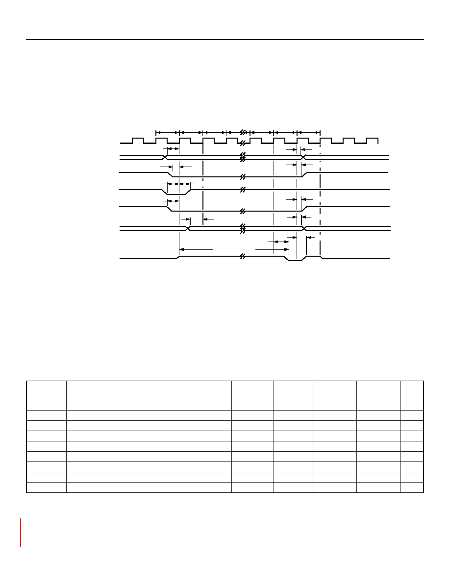
synchronous mode write cycle is given in Figure 7-1 and in Table 7-1, and for the read cycle in Figure 7-2 and in Table 7-2.
Notes:
MPCLK
Input clock to 4565B Ultramapper Full Transport Retiming Device MPU block.
ADDR [20:0]
The address will be available throughout the entire cycle.
CSN (Input)
Chip select is an active-low signal.
ADSN (Input) Address strobe is active-low. ADSN must be one MPCLK clock period wide.
RWN (Input)
The read (H) write (L) signal is always high except during a write cycle.
DATA[15:0]
Data will be available during cycle T1.
DTN (Output) Data transfer acknowledge is active-low for one clock and then driven high before entering a high-impedance state. (This is done with an
I/O pad using the input as feedback to qualify the 3-state term.) DTN will become 3-stated when CSN is high. Typically, DTN is active for
four or five MPCLK cycles after ADSN is low.
Figure 7-1. Microprocessor Interface Synchronous Write Cycle—MPMODE Pin = 1
* If DTN is used, then the maximum frequency for MPCLK is determined by the processor’s setup specification for DTN. MPU maximum bus operating
frequency = 1/(MPU DTN setup time + tDTNVPD). For example, a 8 ns setup time would limit MPCLK to 50 MHz for reliable DTN detection.
DTN fall is variable, depending on the block selected for access and in some cases the state of the SONET frame. This interval is typically in the 100 ns
to 200 ns range, but can be several hundred ns. In lab measurements, it has never exceeded 1000 ns. Certain registers in the VTMPR block have a
very long acknowledge cycle (in the order of 32 MPCLK cycles). The reason for this is that those registers can also be accessed by the VTMPR lower
order path overhead interface as part of SONET overhead termination functions. Therefore, the user must insert long enough delay or use the DTN sig-
nal to read/write these registers correctly.
Table 7-1. Microprocessor Interface Synchronous Write Cycle Specifications
Symbol
Parameter
Setup
(Min)
Hold (Min) Delay (Min) Delay (Max) Unit
MPCLK
MPCLK 16 MHz Min—66* MHz Max Frequency
—
ns
tWS
ADSN, RWN, DATA (write) Valid to MPCLK
6.7
—
——
ns
tAPD
MPCLK to ADDR, RWN, DATA, CSN (write) Invalid
—
0
—
ns
tCSNVS CSN Valid to MPCLK
6
—
ns
tADDRVS ADDR Valid to MPCLK
3.5
—
ns
tAIPD
MPCLK to ADSN Invalid
—
0
—
ns
tDTNVPD MPCLK to DTN Valid
—
2.5
12
ns
tDTNIPD MPCLK to DTN Invalid
—
2.5
12
ns
TADSNVDTF ADSN Valid to DTN Falling
—
—
ns
MPCLK
ADDR[20:0]
CSN
ADSN
RWN
DATA[15:0]
DTN
(INPUT)
tWS
tDTNVPD
tADDRVS
tCSNVS
tWS
T0
T1
T2
T3
Tn – 2
Tn – 1
Tn
tAIPD
tAPD
tDTNIPD
HIGH Z
tADSNVDTF
相關(guān)PDF資料 |
PDF描述 |
|---|---|
| 45APC180K | 1 ELEMENT, 18 uH, GENERAL PURPOSE INDUCTOR |
| 45APC470K | 1 ELEMENT, 47 uH, GENERAL PURPOSE INDUCTOR |
| 45APC272K | 1 ELEMENT, 2700 uH, GENERAL PURPOSE INDUCTOR |
| 45K101-101H3 | CABLE TERMINATED, FEMALE, RF CONNECTOR, CRIMP, JACK |
| 45K101-102H3 | CABLE TERMINATED, FEMALE, RF CONNECTOR, CRIMP, JACK |
相關(guān)代理商/技術(shù)參數(shù) |
參數(shù)描述 |
|---|---|
| 4565-BLK | 制造商:Pomona Electronics 功能描述:ACCESSORIES, MAXIGRABBER TEST CLIP |
| 4565-BLK-3XL | 功能描述:3M DISPOSABLE CHEMICAL PROTE 制造商:3m 系列:* 零件狀態(tài):在售 標(biāo)準(zhǔn)包裝:1 |
| 4565-BLK-4XL | 功能描述:3M DISPOSABLE CHEMICAL PROTE 制造商:3m 系列:* 零件狀態(tài):在售 標(biāo)準(zhǔn)包裝:1 |
| 4565-BLK-L | 功能描述:3M DISPOSABLE CHEMICAL PROTE 制造商:3m 系列:* 零件狀態(tài):在售 標(biāo)準(zhǔn)包裝:1 |
| 4565-BLK-M | 功能描述:3M DISPOSABLE CHEMICAL PROTE 制造商:3m 系列:* 零件狀態(tài):在售 標(biāo)準(zhǔn)包裝:1 |
發(fā)布緊急采購(gòu),3分鐘左右您將得到回復(fù)。