- 您現(xiàn)在的位置:買賣IC網(wǎng) > PDF目錄156622 > 4565B2 ATM/SONET/SDH SUPPORT CIRCUIT, PBGA909 PDF資料下載
參數(shù)資料
| 型號: | 4565B2 |
| 元件分類: | 數(shù)字傳輸電路 |
| 英文描述: | ATM/SONET/SDH SUPPORT CIRCUIT, PBGA909 |
| 封裝: | PLASTIC, BGA-909 |
| 文件頁數(shù): | 33/61頁 |
| 文件大小: | 1691K |
| 代理商: | 4565B2 |
第1頁第2頁第3頁第4頁第5頁第6頁第7頁第8頁第9頁第10頁第11頁第12頁第13頁第14頁第15頁第16頁第17頁第18頁第19頁第20頁第21頁第22頁第23頁第24頁第25頁第26頁第27頁第28頁第29頁第30頁第31頁第32頁當前第33頁第34頁第35頁第36頁第37頁第38頁第39頁第40頁第41頁第42頁第43頁第44頁第45頁第46頁第47頁第48頁第49頁第50頁第51頁第52頁第53頁第54頁第55頁第56頁第57頁第58頁第59頁第60頁第61頁
Hardware Design Guide, Revision 2
4565B Ultramapper Full Transport Retiming Device
December 17, 2003
622/155 Mbits/s SONET/SDH x DS3/E3/DS2/DS1/E1
Agere Systems Inc.
39
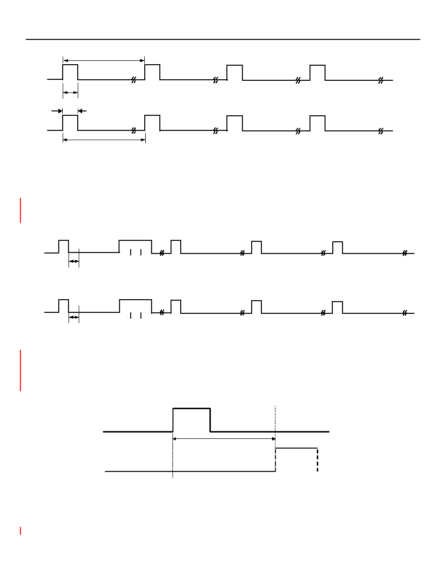
Figure 5-4. THSSYNC Timing Diagram (MPU_MASTER_SLAVE = 0)
When supplied externally, the 8 kHz THSSYNC may have a 50/50 duty cycle since the signal will only be sampled on the
rising edge. In this case, THSSYNC should be synchronous to THSC.
However, if the system needs to synchronize VTs, generated from different Ultramapper FT Retiming devices or other ex-
ternal devices, then THSSYNC needs to look like the waveform representation in Figure 5-5, i.e., THSSYNC must be com-
posed of both the 8 kHz and the 2 kHz sync components (J0 + V1-1—V1-3); the J1 portion is not needed.
Figure 5-5. THSSYNC Timing Diagram for Synchronized VTs
The Figure 5-6 depicts the relationship between the rising edge of the input THSSYNC (when the device is in slave mode)
and the beginning of the SONET frame output on THSD. The delay between THSSYNC and the start of the outgoing SONET
frame is contributed to internal device delays (pertaining to multiplexing functionality, FIFO, and parallel to serial conversion).
Figure 5-6. Relationship Between THSSYNC and THSD
STS-3
J0
FIRST FRAME
50 ns
STS-12
50 ns
125
s
125
s
J0
SECOND FRAME
THIRD FRAME
FOURTH FRAME
SECOND FRAME
THIRD FRAME
FOURTH FRAME
FIRST FRAME
J0
STS-3
J0
V1-1
FIRST FRAME
50 ns
SECOND FRAME
THIRD FRAME
FOURTH FRAME
STS-12
V1-2
V1-3
J0
V1-1
V1-2
V1-3
50 ns
J0
FIRST FRAME
SECOND FRAME
THIRD FRAME
FOURTH FRAME
THSSYNC
THSD
A1
N
622 Mbits/s mode: N = 80 +/- 8 bits
155 Mbits/s mode: N = 44 +/- 8 bits
For the case where TMUX_TLBITCNT, TMUX_TLSTSCNT, TMUX_TLCOLCNT, and TMUX_TLROWCNT all = 0 (default).
Changing these register values will change the location of point X in relation to point Y
X
Y
相關(guān)PDF資料 |
PDF描述 |
|---|---|
| 45APC180K | 1 ELEMENT, 18 uH, GENERAL PURPOSE INDUCTOR |
| 45APC470K | 1 ELEMENT, 47 uH, GENERAL PURPOSE INDUCTOR |
| 45APC272K | 1 ELEMENT, 2700 uH, GENERAL PURPOSE INDUCTOR |
| 45K101-101H3 | CABLE TERMINATED, FEMALE, RF CONNECTOR, CRIMP, JACK |
| 45K101-102H3 | CABLE TERMINATED, FEMALE, RF CONNECTOR, CRIMP, JACK |
相關(guān)代理商/技術(shù)參數(shù) |
參數(shù)描述 |
|---|---|
| 4565-BLK | 制造商:Pomona Electronics 功能描述:ACCESSORIES, MAXIGRABBER TEST CLIP |
| 4565-BLK-3XL | 功能描述:3M DISPOSABLE CHEMICAL PROTE 制造商:3m 系列:* 零件狀態(tài):在售 標準包裝:1 |
| 4565-BLK-4XL | 功能描述:3M DISPOSABLE CHEMICAL PROTE 制造商:3m 系列:* 零件狀態(tài):在售 標準包裝:1 |
| 4565-BLK-L | 功能描述:3M DISPOSABLE CHEMICAL PROTE 制造商:3m 系列:* 零件狀態(tài):在售 標準包裝:1 |
| 4565-BLK-M | 功能描述:3M DISPOSABLE CHEMICAL PROTE 制造商:3m 系列:* 零件狀態(tài):在售 標準包裝:1 |
發(fā)布緊急采購,3分鐘左右您將得到回復。