- 您現(xiàn)在的位置:買賣IC網(wǎng) > PDF目錄297706 > V58C2128804-75L (MOSEL-VITELIC) 16M X 8 DDR DRAM, 0.75 ns, PDSO66 PDF資料下載
參數(shù)資料
| 型號: | V58C2128804-75L |
| 廠商: | MOSEL-VITELIC |
| 元件分類: | DRAM |
| 英文描述: | 16M X 8 DDR DRAM, 0.75 ns, PDSO66 |
| 封裝: | PLASTIC, TSOP2-66 |
| 文件頁數(shù): | 33/58頁 |
| 文件大小: | 722K |
| 代理商: | V58C2128804-75L |
第1頁第2頁第3頁第4頁第5頁第6頁第7頁第8頁第9頁第10頁第11頁第12頁第13頁第14頁第15頁第16頁第17頁第18頁第19頁第20頁第21頁第22頁第23頁第24頁第25頁第26頁第27頁第28頁第29頁第30頁第31頁第32頁當(dāng)前第33頁第34頁第35頁第36頁第37頁第38頁第39頁第40頁第41頁第42頁第43頁第44頁第45頁第46頁第47頁第48頁第49頁第50頁第51頁第52頁第53頁第54頁第55頁第56頁第57頁第58頁
39
MOSEL VITELIC
V58C2128(804/404/164)SAT
V58C2128(804/404/164)SAT Rev. 1.1 February 2001
NOTES: (continued)
23. The refresh period 64ms. This equates to an average refresh rate of 15.625s. However, an AUTO REFRESH
command must be asserted at least once every 140.6s; burst refreshing or posting by the DRAM controller greater
than eight refresh cycles is not allowed.
24. The I/O capacitance per DQS and DQ byte/group will not differ by more than this maximum amount for any
given device.
25. The valid data window is derived by achieving other specifications - tHP (tCK/2), tDQSQ, and tQH
(tQH = tHP - tQHS). The data valid window derates directly porportional with the clock duty cycle and a practical data
valid window can be derived. The clock is allowed a maximum duty cycle variation of 45/55. Functionality is uncertain
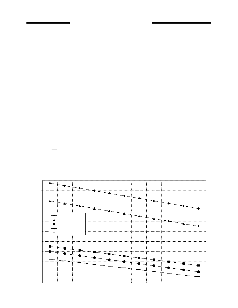
when operating beyond a 45/55 ratio. The data valid window derating curves are provided below for duty cycles rang-
ing between 50/50 and 45/55.
26. Referenced to each output group: x4 = DQS with DQ0-DQ3; x8 = DQS with DQ0-DQ7; x16 = LDQS with DQ0-
DQ7; and UDQS with DQ8-DQ15.
27. This limit is actually a nominal value and does not result in a fail value. CKE is HIGH during REFRESH command
period (tRFC [MIN]) else CKE is LOW (i.e., during standby).
28. To maintain a valid level, the transitioning edge of the input must:
a) Sustain a constant slew rate from the current AC level through to the target AC level, VIL(AC) or VIH(AC).
b) Reach at least the target AC level.
c) After the AC target level is reached, continue to maintain at least the target DC level, VIL(DC) or VIH(DC).
29. The Input capacitance per pin group will not differ by more than this maximum amount for any given device..
30. CK and CK input slew rate must be 1V/ns.
31. DQ and DM input slew rates must not deviate from DQS by more than 10%. If the DQ/DM/DQS slew rate is less
than 0.5V/ns, timing must be derated: 50ps must be added to tDS and tDH for each 100mv/ns reduction in slew rate.
If slew rate exceeds 4V/ns, functionality is uncertain.
32. VDD must not vary more than 4% if CKE is not active while any bank is active.
3.8
3.750
3.700
3.650
3.600
3.550
3.500
3.450
3.400
3.350
3.300
3.250
3.400
50/50
49.5/50.5
49/51
48.5/52.5
48/52
47.5/53.5
47/53
46.5/54.5
46/54
45.5/55.5
45/55
2.463
2.500
2.425
2.388
2.350
2.313
2.275
2.238
2.200
2.163
2.125
3.350
3.300
3.250
3.200
3.150
3.100
3.050
3.000
2.950
2.900
3.6
3.4
3.2
3.0
2.8
2.6
2.4
2.2
2.0
1.8
-7, -75 @tCK = 10ns
-8, @tCK = 10ns
-7, -75 @tCK = 7.5ns
-8, @tCK = 8ns
-7, @tCK = 7ns
ns
相關(guān)PDF資料 |
PDF描述 |
|---|---|
| V58C2256324SAH-40 | 8M X 32 DDR DRAM, 0.6 ns, PBGA144 |
| V59C1512404QBLF3I | 128M X 4 DDR DRAM, 0.45 ns, PBGA60 |
| V5A010CB3H | SNAP ACTING/LIMIT SWITCH, SPDT, MOMENTARY, 0.6A, 125VDC, 4.4mm, PANEL MOUNT |
| V5B010FB3 | SNAP ACTING/LIMIT SWITCH, SPDT, MOMENTARY, 2.3mm, PANEL MOUNT |
| V5B030CB3H | SNAP ACTING/LIMIT SWITCH, SPST, MOMENTARY, 0.6A, 125VDC, 4.4mm, PANEL MOUNT |
相關(guān)代理商/技術(shù)參數(shù) |
參數(shù)描述 |
|---|---|
| V58C2128804S | 制造商:MOSEL 制造商全稱:MOSEL 功能描述:HIGH PERFORMANCE 2.5 VOLT 128 Mbit DDR SDRAM |
| V58C2256 | 制造商:MOSEL 制造商全稱:MOSEL 功能描述:HIGH PERFORMANCE 2.5 VOLT 256 Mbit DDR SDRAM |
| V58C2256164S | 制造商:MOSEL 制造商全稱:MOSEL 功能描述:HIGH PERFORMANCE 2.5 VOLT 256 Mbit DDR SDRAM |
| V58C2256324SAB30 | 制造商:Marvell 功能描述:Marvell V58C2256324SAB30 |
| V58C2256324SAB33 | 制造商:Marvell 功能描述:Marvell V58C2256324SAB33 |
發(fā)布緊急采購,3分鐘左右您將得到回復(fù)。