- 您現(xiàn)在的位置:買賣IC網(wǎng) > PDF目錄385949 > TSB42AB4I (Texas Instruments, Inc.) IEEE 1394 A CONSUMER ELECTRONICS LINK LAYER CONTROLLER PDF資料下載
參數(shù)資料
| 型號: | TSB42AB4I |
| 廠商: | Texas Instruments, Inc. |
| 英文描述: | IEEE 1394 A CONSUMER ELECTRONICS LINK LAYER CONTROLLER |
| 中文描述: | 1394消費(fèi)電子產(chǎn)品鏈路層控制器 |
| 文件頁數(shù): | 144/183頁 |
| 文件大?。?/td> | 798K |
| 代理商: | TSB42AB4I |
第1頁第2頁第3頁第4頁第5頁第6頁第7頁第8頁第9頁第10頁第11頁第12頁第13頁第14頁第15頁第16頁第17頁第18頁第19頁第20頁第21頁第22頁第23頁第24頁第25頁第26頁第27頁第28頁第29頁第30頁第31頁第32頁第33頁第34頁第35頁第36頁第37頁第38頁第39頁第40頁第41頁第42頁第43頁第44頁第45頁第46頁第47頁第48頁第49頁第50頁第51頁第52頁第53頁第54頁第55頁第56頁第57頁第58頁第59頁第60頁第61頁第62頁第63頁第64頁第65頁第66頁第67頁第68頁第69頁第70頁第71頁第72頁第73頁第74頁第75頁第76頁第77頁第78頁第79頁第80頁第81頁第82頁第83頁第84頁第85頁第86頁第87頁第88頁第89頁第90頁第91頁第92頁第93頁第94頁第95頁第96頁第97頁第98頁第99頁第100頁第101頁第102頁第103頁第104頁第105頁第106頁第107頁第108頁第109頁第110頁第111頁第112頁第113頁第114頁第115頁第116頁第117頁第118頁第119頁第120頁第121頁第122頁第123頁第124頁第125頁第126頁第127頁第128頁第129頁第130頁第131頁第132頁第133頁第134頁第135頁第136頁第137頁第138頁第139頁第140頁第141頁第142頁第143頁當(dāng)前第144頁第145頁第146頁第147頁第148頁第149頁第150頁第151頁第152頁第153頁第154頁第155頁第156頁第157頁第158頁第159頁第160頁第161頁第162頁第163頁第164頁第165頁第166頁第167頁第168頁第169頁第170頁第171頁第172頁第173頁第174頁第175頁第176頁第177頁第178頁第179頁第180頁第181頁第182頁第183頁
647
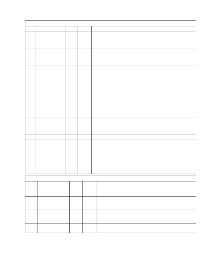
0x150 DBINT0EN Data Buffer Interrupt 0 Enables (Continued)
BIT
NAME
TYPE
RESET
FUNCTION
8
BUF1EMPTY
RW
0
Buffer 1 empty When this bit is set to 1, the SYSINT.DBINT0 bit is set to
1 when the corresponding bit in the DBINT0 register is set by hardware.
When set to 0, the corresponding bit in the DBINT0 register has no effect
on the SYSINT.DBINT0 bit.
7
BUF0CELLCFRM
RW
0
Buffer 0 cell confirm When this bit is set to 1, the SYSINT.DBINT0 bit is
set to 1 when the corresponding bit in the DBINT0 register is set by
hardware. When set to 0, the corresponding bit in the DBINT0 register
has no effect on the SYSINT.DBINT0 bit.
6
BUF0TSREL
RW
0
Buffer 0 time stamp release When this bit is set to 1, the
SYSINT.DBINT0 bit is set to 1 when the corresponding bit in the DBINT0
register is set by hardware. When set to 0, the corresponding bit in the
DBINT0 register has no effect on the SYSINT.DBINT0 bit.
5
BUF0AGED
RW
0
Buffer 0 time stamp expired When this bit is set to 1, the
SYSINT.DBINT0 bit is set to 1 when the corresponding bit in the DBINT0
register is set by hardware. When set to 0, the corresponding bit in the
DBINT0 register has no effect on the SYSINT.DBINT0 bit.
4
BUF0WM1
RW
0
Buffer 0 water mark 1 When this bit is set to 1, the SYSINT.DBINT0 bit
is set to 1 when the corresponding bit in the DBINT0 register is set by
hardware. When set to 0, the corresponding bit in the DBINT0 register
has no effect on the SYSINT.DBINT0 bit.
3
BUF0WM0
RW
0
Buffer 0 water mark 0 When this bit is set to 1, the SYSINT.DBINT0 bit
is set to 1 when the corresponding bit in the DBINT0 register is set by
hardware. When set to 0, the corresponding bit in the DBINT0 register
has no effect on the SYSINT.DBINT0 bit.
2
RSVD
R0
0
Reserved – A write to this location has no effect. A read returns 0.
1
BUF0FULL
RW
0
Buffer 0 full When this bit is set to 1, the SYSINT.DBINT0 bit is set to 1
when the corresponding bit in the DBINT0 register is set by hardware.
When set to 0, the corresponding bit in the DBINT0 register has no effect
on the SYSINT.DBINT0 bit.
0
BUF0EMPTY
RW
0
Buffer 0 empty When this bit is set to 1, the SYSINT.DBINT0 bit is set to
1 when the corresponding bit in the DBINT0 register is set by hardware.
When set to 0, the corresponding bit in the DBINT0 register has no effect
on the SYSINT.DBINT0 bit.
0x154 DBINT1 – Data Buffer Interrupts 1
BIT
NAME
TYPE
RESET
FUNCTION
31
BUF7CELLCFRM
RCU
0
Buffer 7 cell confirm – This bit is set by hardware to indicate that a
complete logical cell has been confirmed into the associated buffer.
30
BUF7TSREL
RCU
0
Buffer 7 time stamp release – This bit is set by hardware to indicate
that a time-stamped logical cell in the current buffer is ready to be
released, irrespective of buffer direction.
29
BUF7AGED
RCU
0
Buffer 7 time stamp expired – This bit is set by hardware to indicate
that a time-stamped logical cell in the current buffer has been flushed
because its time stamp expired, irrespective of buffer direction.
28
BUF7WM1
RCU
0
Buffer 7 water mark 1 This bit is set by hardware to indicate that
DBSTAT1.BUF7WM1 has changed its status from 0 to 1.
相關(guān)PDF資料 |
PDF描述 |
|---|---|
| TSB42AB4PGE | IEEE 1394 A CONSUMER ELECTRONICS LINK LAYER CONTROLLER |
| TSB43AA82A1 | 1394 integrated PHY and link layer controller(1394集成PHY和鏈路層控制器) |
| TSB81BA3I | IEEE 1394b THREE-PORT CABLE TRANSCEIVER/ARBITER |
| TSE-0155-32S-P1-3 | SINGLE MODE SINGLE FIBER TRANSCEIVER |
| TSL230 | PROGRAMMABLE LIGHT-TO-FREQUENCY CONVERTERS |
相關(guān)代理商/技術(shù)參數(shù) |
參數(shù)描述 |
|---|---|
| TSB42AB4IPDT | 功能描述:1394 接口集成電路 1394 Link Layer Cntrlr RoHS:否 制造商:Texas Instruments 類型:Link Layer Controller 工作電源電壓: 封裝 / 箱體:LQFP 封裝:Tray |
| TSB42AB4PDT | 功能描述:1394 接口集成電路 1394 Link Layer Cntrlr RoHS:否 制造商:Texas Instruments 類型:Link Layer Controller 工作電源電壓: 封裝 / 箱體:LQFP 封裝:Tray |
| TSB42AB4PDTG4 | 功能描述:1394 接口集成電路 Link Layer Cntrlr RoHS:否 制造商:Texas Instruments 類型:Link Layer Controller 工作電源電壓: 封裝 / 箱體:LQFP 封裝:Tray |
| TSB42AB4PGE | 制造商:TI 制造商全稱:Texas Instruments 功能描述:IEEE 1394 A CONSUMER ELECTRONICS LINK LAYER CONTROLLER |
| TSB42AC3 | 制造商:TI 制造商全稱:Texas Instruments 功能描述:General purpose link layer ideal for a wide-range of applications |
發(fā)布緊急采購,3分鐘左右您將得到回復(fù)。