- 您現(xiàn)在的位置:買(mǎi)賣(mài)IC網(wǎng) > PDF目錄383961 > TMX320DM6443AZWT (Texas Instruments, Inc.) Digital Media System-on-Chip PDF資料下載
參數(shù)資料
| 型號(hào): | TMX320DM6443AZWT |
| 廠商: | Texas Instruments, Inc. |
| 英文描述: | Digital Media System-on-Chip |
| 中文描述: | 數(shù)字媒體系統(tǒng)片上 |
| 文件頁(yè)數(shù): | 59/221頁(yè) |
| 文件大?。?/td> | 1582K |
| 代理商: | TMX320DM6443AZWT |
第1頁(yè)第2頁(yè)第3頁(yè)第4頁(yè)第5頁(yè)第6頁(yè)第7頁(yè)第8頁(yè)第9頁(yè)第10頁(yè)第11頁(yè)第12頁(yè)第13頁(yè)第14頁(yè)第15頁(yè)第16頁(yè)第17頁(yè)第18頁(yè)第19頁(yè)第20頁(yè)第21頁(yè)第22頁(yè)第23頁(yè)第24頁(yè)第25頁(yè)第26頁(yè)第27頁(yè)第28頁(yè)第29頁(yè)第30頁(yè)第31頁(yè)第32頁(yè)第33頁(yè)第34頁(yè)第35頁(yè)第36頁(yè)第37頁(yè)第38頁(yè)第39頁(yè)第40頁(yè)第41頁(yè)第42頁(yè)第43頁(yè)第44頁(yè)第45頁(yè)第46頁(yè)第47頁(yè)第48頁(yè)第49頁(yè)第50頁(yè)第51頁(yè)第52頁(yè)第53頁(yè)第54頁(yè)第55頁(yè)第56頁(yè)第57頁(yè)第58頁(yè)當(dāng)前第59頁(yè)第60頁(yè)第61頁(yè)第62頁(yè)第63頁(yè)第64頁(yè)第65頁(yè)第66頁(yè)第67頁(yè)第68頁(yè)第69頁(yè)第70頁(yè)第71頁(yè)第72頁(yè)第73頁(yè)第74頁(yè)第75頁(yè)第76頁(yè)第77頁(yè)第78頁(yè)第79頁(yè)第80頁(yè)第81頁(yè)第82頁(yè)第83頁(yè)第84頁(yè)第85頁(yè)第86頁(yè)第87頁(yè)第88頁(yè)第89頁(yè)第90頁(yè)第91頁(yè)第92頁(yè)第93頁(yè)第94頁(yè)第95頁(yè)第96頁(yè)第97頁(yè)第98頁(yè)第99頁(yè)第100頁(yè)第101頁(yè)第102頁(yè)第103頁(yè)第104頁(yè)第105頁(yè)第106頁(yè)第107頁(yè)第108頁(yè)第109頁(yè)第110頁(yè)第111頁(yè)第112頁(yè)第113頁(yè)第114頁(yè)第115頁(yè)第116頁(yè)第117頁(yè)第118頁(yè)第119頁(yè)第120頁(yè)第121頁(yè)第122頁(yè)第123頁(yè)第124頁(yè)第125頁(yè)第126頁(yè)第127頁(yè)第128頁(yè)第129頁(yè)第130頁(yè)第131頁(yè)第132頁(yè)第133頁(yè)第134頁(yè)第135頁(yè)第136頁(yè)第137頁(yè)第138頁(yè)第139頁(yè)第140頁(yè)第141頁(yè)第142頁(yè)第143頁(yè)第144頁(yè)第145頁(yè)第146頁(yè)第147頁(yè)第148頁(yè)第149頁(yè)第150頁(yè)第151頁(yè)第152頁(yè)第153頁(yè)第154頁(yè)第155頁(yè)第156頁(yè)第157頁(yè)第158頁(yè)第159頁(yè)第160頁(yè)第161頁(yè)第162頁(yè)第163頁(yè)第164頁(yè)第165頁(yè)第166頁(yè)第167頁(yè)第168頁(yè)第169頁(yè)第170頁(yè)第171頁(yè)第172頁(yè)第173頁(yè)第174頁(yè)第175頁(yè)第176頁(yè)第177頁(yè)第178頁(yè)第179頁(yè)第180頁(yè)第181頁(yè)第182頁(yè)第183頁(yè)第184頁(yè)第185頁(yè)第186頁(yè)第187頁(yè)第188頁(yè)第189頁(yè)第190頁(yè)第191頁(yè)第192頁(yè)第193頁(yè)第194頁(yè)第195頁(yè)第196頁(yè)第197頁(yè)第198頁(yè)第199頁(yè)第200頁(yè)第201頁(yè)第202頁(yè)第203頁(yè)第204頁(yè)第205頁(yè)第206頁(yè)第207頁(yè)第208頁(yè)第209頁(yè)第210頁(yè)第211頁(yè)第212頁(yè)第213頁(yè)第214頁(yè)第215頁(yè)第216頁(yè)第217頁(yè)第218頁(yè)第219頁(yè)第220頁(yè)第221頁(yè)
www.ti.com
3
Device Configurations
3.1 System Module Registers
3.2 Power Considerations
3.2.1
Power Configurations at Reset
TMS320DM6443
Digital Media System-on-Chip
SPRS282E–DECEMBER 2005–REVISED MARCH 2007
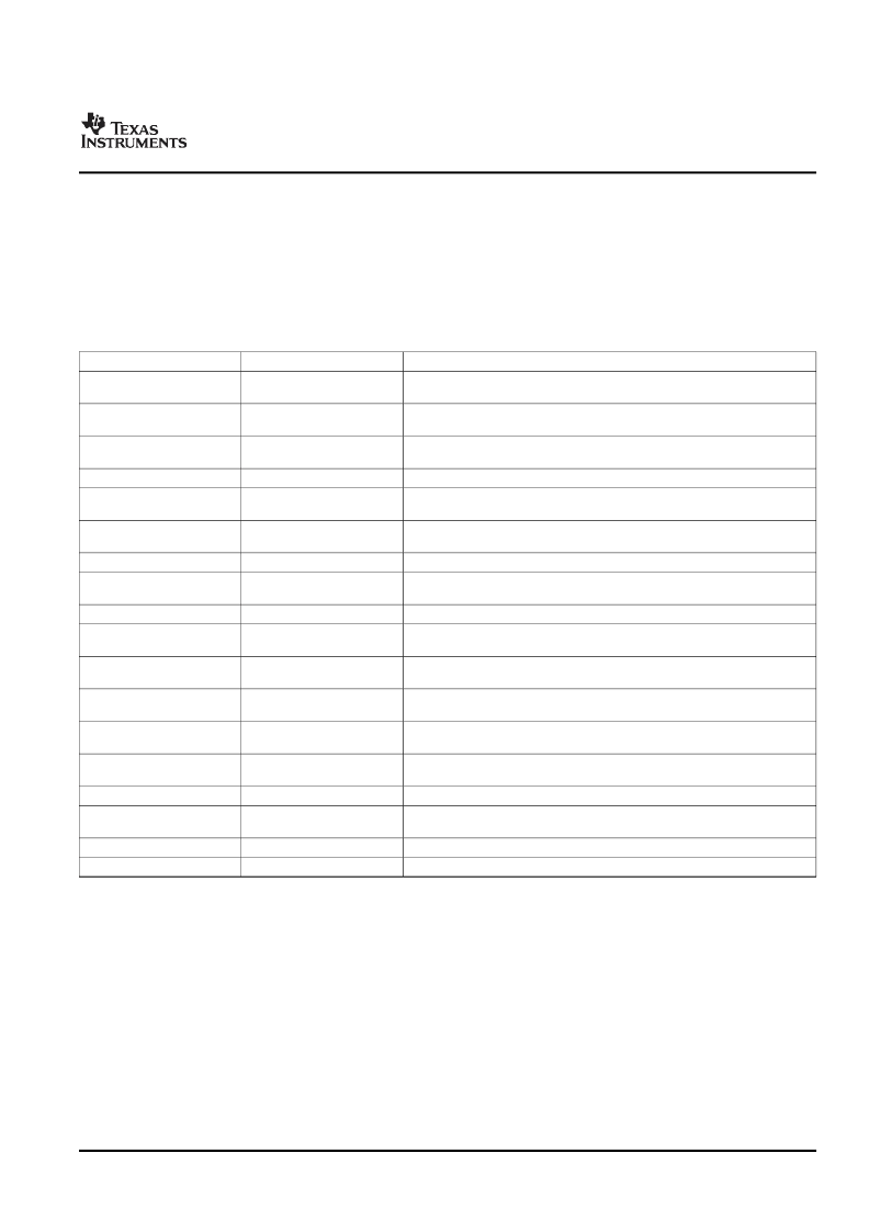
The system module includes status and control registers required for configuration of the device. Brief
descriptions of the various registers are shown in
Table 3-1
. System Module registers required for device
configurations are discussed in the following sections.
Table 3-1. System Module Register Memory Map
HEX ADDRESS RANGE
0x01C4 0000
REGISTER ACRONYM
PINMUX0
DESCRIPTION
Pin multiplexing control 0. For details, see
Section 3.5.4
, PINMUX0 Register
Description.
Pin multiplexing control 1. For details, see
Section 3.5.5
, PINMUX1 Register
Description.
Boot address of DSP. For details, see
Section 3.3.1.2
, DSPBOOTADDR
Register Description.
Emulator Suspend Source. For details, see
Section 3.6
, Emulation Control.
ARM/DSP Interrupt Status and Control. For details, see
Section 6.7.3
,
ARM/DSP Communications Interrupts.
Device boot configuration. For details, see
Section 3.3.1.1
, BOOTCFG
Register Description.
Reserved.
JTAGID/Device ID number. For details, see
Section 6.25.1
, JTAG ID Register
Description.
Reserved.
HPI control. For details, see
Section 3.5.6.10
, HPI and EMIFA/ATA Pin
Multiplexing.
USB PHY control. For details, see
Section 6.15.1
, USBPHY_CTL Register
Description.
Chip shorting switch control. For details, see
Section 3.2.1
, Power
Configurations at Reset.
Bus master priority control 0. For details, see
Section 3.5.1
, Switched Central
Resource (SCR) Bus Priorities.
Bus master priority control 1. For details, see
Section 3.5.1
, Switched Central
Resource (SCR) Bus Priorities.
VPSS clock control.
VDD 3.3V I/O powerdown control. For details, see
Section 3.2.2
, Power
Configurations after Reset.
Enables access to the DDR2 VTP Register.
Reserved.
0x01C4 0004
PINMUX1
0x01C4 0008
DSPBOOTADDR
0x01C4 000C
0x01C4 0010
SUSPSRC
INTGEN
0x01C4 0014
BOOTCFG
0x01C4 0018 - 0x01C4 0027
0x01C4 0028
–
JTAGID
0x01C4 002C
0x01C4 0030
–
HPI_CTL
0x01C4 0034
USBPHY_CTL
0x01C4 0038
CHP_SHRTSW
0x01C4 003C
MSTPRI0
0x01C4 0040
MSTPRI1
0x01C4 0044
0x01C4 0048
VPSS_CLKCTL
VDD3P3V_PWDN
0x01C4 004C
DRRVTPER
–
0x01C4 0050 - 0x01C4 006F
Global device power domains are controlled by the Power and Sleep Controller, except as shown in the
following sections.
As described in the
DM6443 Power and Clock Domains
section, the DM6443 has two power domains:
Always On and DSP. There is a shorting switch between the two power domains that must be opened
when the DSP domain is powered off and closed when the DSP domain is powered on.
The CHP_SHRTSW register, shown in
Figure 3-1
, controls the shorting switch between the device
always-on and DSP power domains. This switch should be enabled after powering-up the DSP domain.
Submit Documentation Feedback
Device Configurations
59
相關(guān)PDF資料 |
PDF描述 |
|---|---|
| TMX320DM6443ZWT | Digital Media System-on-Chip |
| TMS320DM647_08 | Digital Media Processor |
| TMS320DM647ZUT720 | Digital Media Processor |
| TMS320DM647ZUT900 | Digital Media Processor |
| TMS320DM648ZUT720 | Digital Media Processor |
相關(guān)代理商/技術(shù)參數(shù) |
參數(shù)描述 |
|---|---|
| TMX320DM6443BZWT | 制造商:Texas Instruments 功能描述: |
| TMX320DM6443CZWT | 制造商:Texas Instruments 功能描述: |
| TMX320DM6443ZWT | 制造商:Texas Instruments 功能描述: |
| TMX320DM6444AZWT | 制造商:Texas Instruments 功能描述:TMS320DM6443, TMS320DM6444 DIGITAL MEDIA SOC DATA SHEET - Trays |
| TMX320DM6446AZWT | 制造商:Texas Instruments 功能描述: |
發(fā)布緊急采購(gòu),3分鐘左右您將得到回復(fù)。