- 您現(xiàn)在的位置:買(mǎi)賣(mài)IC網(wǎng) > PDF目錄383961 > TMX320DM6443AZWT (Texas Instruments, Inc.) Digital Media System-on-Chip PDF資料下載
參數(shù)資料
| 型號(hào): | TMX320DM6443AZWT |
| 廠商: | Texas Instruments, Inc. |
| 英文描述: | Digital Media System-on-Chip |
| 中文描述: | 數(shù)字媒體系統(tǒng)片上 |
| 文件頁(yè)數(shù): | 131/221頁(yè) |
| 文件大小: | 1582K |
| 代理商: | TMX320DM6443AZWT |
第1頁(yè)第2頁(yè)第3頁(yè)第4頁(yè)第5頁(yè)第6頁(yè)第7頁(yè)第8頁(yè)第9頁(yè)第10頁(yè)第11頁(yè)第12頁(yè)第13頁(yè)第14頁(yè)第15頁(yè)第16頁(yè)第17頁(yè)第18頁(yè)第19頁(yè)第20頁(yè)第21頁(yè)第22頁(yè)第23頁(yè)第24頁(yè)第25頁(yè)第26頁(yè)第27頁(yè)第28頁(yè)第29頁(yè)第30頁(yè)第31頁(yè)第32頁(yè)第33頁(yè)第34頁(yè)第35頁(yè)第36頁(yè)第37頁(yè)第38頁(yè)第39頁(yè)第40頁(yè)第41頁(yè)第42頁(yè)第43頁(yè)第44頁(yè)第45頁(yè)第46頁(yè)第47頁(yè)第48頁(yè)第49頁(yè)第50頁(yè)第51頁(yè)第52頁(yè)第53頁(yè)第54頁(yè)第55頁(yè)第56頁(yè)第57頁(yè)第58頁(yè)第59頁(yè)第60頁(yè)第61頁(yè)第62頁(yè)第63頁(yè)第64頁(yè)第65頁(yè)第66頁(yè)第67頁(yè)第68頁(yè)第69頁(yè)第70頁(yè)第71頁(yè)第72頁(yè)第73頁(yè)第74頁(yè)第75頁(yè)第76頁(yè)第77頁(yè)第78頁(yè)第79頁(yè)第80頁(yè)第81頁(yè)第82頁(yè)第83頁(yè)第84頁(yè)第85頁(yè)第86頁(yè)第87頁(yè)第88頁(yè)第89頁(yè)第90頁(yè)第91頁(yè)第92頁(yè)第93頁(yè)第94頁(yè)第95頁(yè)第96頁(yè)第97頁(yè)第98頁(yè)第99頁(yè)第100頁(yè)第101頁(yè)第102頁(yè)第103頁(yè)第104頁(yè)第105頁(yè)第106頁(yè)第107頁(yè)第108頁(yè)第109頁(yè)第110頁(yè)第111頁(yè)第112頁(yè)第113頁(yè)第114頁(yè)第115頁(yè)第116頁(yè)第117頁(yè)第118頁(yè)第119頁(yè)第120頁(yè)第121頁(yè)第122頁(yè)第123頁(yè)第124頁(yè)第125頁(yè)第126頁(yè)第127頁(yè)第128頁(yè)第129頁(yè)第130頁(yè)當(dāng)前第131頁(yè)第132頁(yè)第133頁(yè)第134頁(yè)第135頁(yè)第136頁(yè)第137頁(yè)第138頁(yè)第139頁(yè)第140頁(yè)第141頁(yè)第142頁(yè)第143頁(yè)第144頁(yè)第145頁(yè)第146頁(yè)第147頁(yè)第148頁(yè)第149頁(yè)第150頁(yè)第151頁(yè)第152頁(yè)第153頁(yè)第154頁(yè)第155頁(yè)第156頁(yè)第157頁(yè)第158頁(yè)第159頁(yè)第160頁(yè)第161頁(yè)第162頁(yè)第163頁(yè)第164頁(yè)第165頁(yè)第166頁(yè)第167頁(yè)第168頁(yè)第169頁(yè)第170頁(yè)第171頁(yè)第172頁(yè)第173頁(yè)第174頁(yè)第175頁(yè)第176頁(yè)第177頁(yè)第178頁(yè)第179頁(yè)第180頁(yè)第181頁(yè)第182頁(yè)第183頁(yè)第184頁(yè)第185頁(yè)第186頁(yè)第187頁(yè)第188頁(yè)第189頁(yè)第190頁(yè)第191頁(yè)第192頁(yè)第193頁(yè)第194頁(yè)第195頁(yè)第196頁(yè)第197頁(yè)第198頁(yè)第199頁(yè)第200頁(yè)第201頁(yè)第202頁(yè)第203頁(yè)第204頁(yè)第205頁(yè)第206頁(yè)第207頁(yè)第208頁(yè)第209頁(yè)第210頁(yè)第211頁(yè)第212頁(yè)第213頁(yè)第214頁(yè)第215頁(yè)第216頁(yè)第217頁(yè)第218頁(yè)第219頁(yè)第220頁(yè)第221頁(yè)
www.ti.com
TMS320DM6443
Digital Media System-on-Chip
SPRS282E–DECEMBER 2005–REVISED MARCH 2007
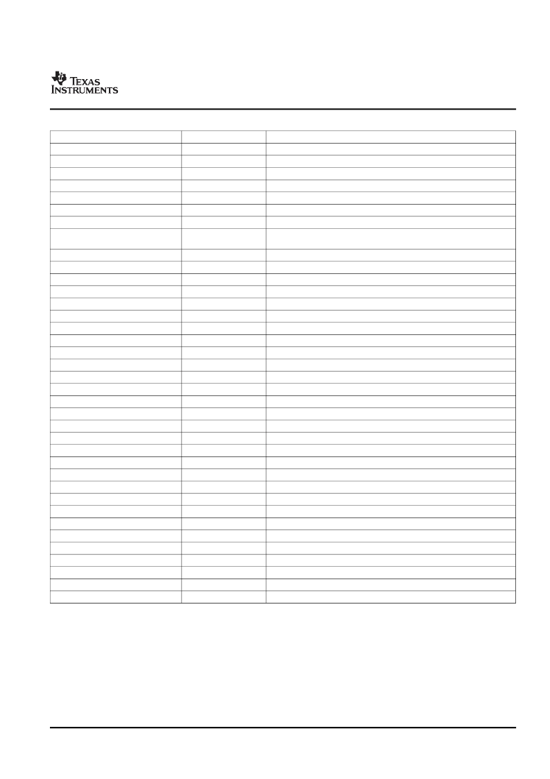
Table 6-30. DM6443 EDMA Registers
(continued)
HEX ADDRESS
0x01c1 0654
0x01c1 0658
0x01c1 065C
0x01c1 0660
0x01c1 0664 - 0x01c1 067F
0x01c1 0680
0x01c1 0684
ACRONYM
SAMPPRXY
SACNTRLD
SASRCBREF
SADSTBREF
-
DFCNTRLD
DFSRCBREF
REGISTER NAME
EDMA3 TC1 Source Active Memory Protection Proxy Register
EDMA3 TC1 Source Active Count Reload Register
EDMA3 TC1 Source Active Source Address B-Reference Register
EDMA3 TC1 Source Active Destination Address B-Reference Register
Reserved
EDMA3 TC1 Destination FIFO Set Count Reload Register
EDMA3 TC1 Destination FIFO Set Source Address B-Reference Register
EDMA3 TC1 Destination FIFO Set Destination Address B-Reference
Register
Reserved
EDMA3 TC1 Destination FIFO Options Register 0
EDMA3 TC1 Destination FIFO Source Address Register 0
EDMA3 TC1 Destination FIFO Count Register 0
EDMA3 TC1 Destination FIFO Destination Address Register 0
EDMA3 TC1 Destination FIFO BIDX Register 0
EDMA3 TC1 Destination FIFO Memory Protection Proxy Register 0
Reserved
EDMA3 TC1 Destination FIFO Options Register 1
EDMA3 TC1 Destination FIFO Source Address Register 1
EDMA3 TC1 Destination FIFO Count Register 1
EDMA3 TC1 Destination FIFO Destination Address Register 1
EDMA3 TC1 Destination FIFO BIDX Register 1
EDMA3 TC1 Destination FIFO Memory Protection Proxy Register 1
Reserved
EDMA3 TC1 Destination FIFO Options Register 2
EDMA3 TC1 Destination FIFO Source Address Register 2
EDMA3 TC1 Destination FIFO Count Register 2
EDMA3 TC1 Destination FIFO Destination Address Register 2
EDMA3 TC1 Destination FIFO BIDX Register 2
EDMA3 TC1 Destination FIFO Memory Protection Proxy Register 2
Reserved
EDMA3 TC1 Destination FIFO Options Register 3
EDMA3 TC1 Destination FIFO Source Address Register 3
EDMA3 TC1 Destination FIFO Count Register 3
EDMA3 TC1 Destination FIFO Destination Address Register 3
EDMA3 TC1 Destination FIFO BIDX Register 3
EDMA3 TC1 Destination FIFO Memory Protection Proxy Register 3
Reserved
0x01c1 0688
DFDSTBREF
0x01c1 068C - 0x01c1 06FF
0x01c1 0700
0x01c1 0704
0x01c1 0708
0x01c1 070C
0x01c1 0710
0x01c1 0714
0x01c1 0718 - 0x01c1 073F
0x01c1 0740
0x01c1 0744
0x01c1 0748
0x01c1 074C
0x01c1 0750
0x01c1 0754
0x01c1 0758 - 0x01c1 077F
0x01c1 0780
0x01c1 0784
0x01c1 0788
0x01c1 078C
0x01c1 0790
0x01c1 0794
0x01c1 0798 - 0x01c1 07BF
0x01c1 07C0
0x01c1 07C4
0x01c1 07C8
0x01c1 07CC
0x01c1 07D0
0x01c1 07D4
0x01c1 07D8 - 0x01c1 07FF
-
DFOPT0
DFSRC0
DFCNT0
DFDST0
DFBIDX0
DFMPPRXY0
-
DFOPT1
DFSRC1
DFCNT1
DFDST1
DFBIDX1
DFMPPRXY1
-
DFOPT2
DFSRC2
DFCNT2
DFDST2
DFBIDX2
DFMPPRXY2
-
DFOPT3
DFSRC3
DFCNT3
DFDST3
DFBIDX3
DFMPPRXY3
-
Table 6-31
shows an abbreviation of the set of registers which make up the parameter set for each of 128
EDMA events. Each of the parameter register sets consist of 8 32-bit word entries.
Table 6-32
shows the
parameter set entry registers with relative memory address locations within each of the parameter sets.
Submit Documentation Feedback
Peripheral and Electrical Specifications
131
相關(guān)PDF資料 |
PDF描述 |
|---|---|
| TMX320DM6443ZWT | Digital Media System-on-Chip |
| TMS320DM647_08 | Digital Media Processor |
| TMS320DM647ZUT720 | Digital Media Processor |
| TMS320DM647ZUT900 | Digital Media Processor |
| TMS320DM648ZUT720 | Digital Media Processor |
相關(guān)代理商/技術(shù)參數(shù) |
參數(shù)描述 |
|---|---|
| TMX320DM6443BZWT | 制造商:Texas Instruments 功能描述: |
| TMX320DM6443CZWT | 制造商:Texas Instruments 功能描述: |
| TMX320DM6443ZWT | 制造商:Texas Instruments 功能描述: |
| TMX320DM6444AZWT | 制造商:Texas Instruments 功能描述:TMS320DM6443, TMS320DM6444 DIGITAL MEDIA SOC DATA SHEET - Trays |
| TMX320DM6446AZWT | 制造商:Texas Instruments 功能描述: |
發(fā)布緊急采購(gòu),3分鐘左右您將得到回復(fù)。